
CHIPS Announces Details on Funding Opportunity Timing
The Department of Commerce (DoC) has announced details regarding funding opportunities and application processes.
- In late February, the DoC plans to release a Notice of Funding Opportunity for commercial leading-edge, current, and mature node fabrication facilities. This includes both “front-end” semiconductor manufacturers and “back-end” packaging facilities.
- In late spring, the DoC plans to release another funding announcement focused on material suppliers and equipment manufacturers.
- In early fall, the DoC plans to announce a funding opportunity to support the construction of semiconductor R&D facilities that will further strengthen the U.S. semiconductor manufacturing ecosystem.
- These announcements will contain detailed guidance, processes, and timelines for organizations to apply for CHIPS incentives.
Let’s now take a look at the updates to the CHIPS Act as detailed by the IAC (Industrial Advisory Council) being run by NIST in the DoC.
CHIPS IAC Feb 2023
There was a recent public meeting of the CHIPS Industrial Advisory Committee (IAC). The IAC is chartered to provide advice on the science and technology needs of the nation’s domestic microelectronics industry, the national strategy on microelectronics research, the research and development programs and other advanced microelectronics activities funded through CHIPS for America, and opportunities for new public-private partnerships.
Dr. Laurie Locasio, Director of NIST and Under Sect of Commerce for Standards and Technology gave some stirring introductory remarks.
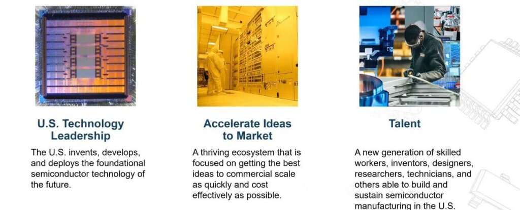
This was followed by Eric Lin, Interim Director of the CHIPS R&D group. He started off by reiterating the overall goals (Figure 1).
IFTLE thinks the most important statement that was made was that the impact of the CHIPS R&D program is maximized when integrated with programs across the USG agencies such as DOD etc……., to realize this integration.
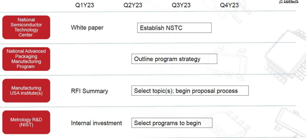
The expected program development timeline is shown below.
National Semiconductor Technology Center (NSTC)
The NSTC will serve as the focal point for research and engineering throughout the semiconductor ecosystem, advancing and enabling disruptive innovation to provide U.S. leadership in the industries of the future. It will be structured as a public-private consortium as an independent entity with a governing board informed and advised by industry, academia, government, and key stakeholders.
It will function as a core of centrally operated, in-house research, engineering, and program capabilities combined with a network of directly funded and affiliated entities.
It will focus research and engineering on challenging projects with a time horizon beyond 5 years.
An NSTC white paper, outlining a governance structure, and describing a preliminary operating and financial model is due out in the 1Q of 2023.
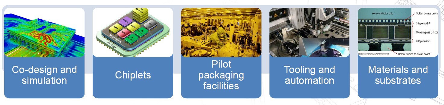
The Advanced Packaging Effort (APE)
The advanced packaging effort is labeled the National Advanced Packaging Manufacturing Program (NAPMP). Quite a mouthful to create an acronym that really isn’t pronounceable. IFTLE would have called it APE!
Its goals are to :
- Create an R&D environment advancing the state-of-the-art in advanced packaging.
- Make investments to bolster the growth in domestic capacity and enhance capabilities for a competitive edge
Thee initial focus is shown in Figure 3.
R&D Gaps Working Group
Dan Armbrust then updated the audience on the efforts of the R&D Gaps Working Group. This group’s charter is to examine the semiconductor industry’s long-term research needs. This working group will then need to understand what is being funded by other government initiatives, where the gaps are, and then suggest priorities to the IAC as to where the focus areas should be for CHIPS funding and the NSTC that provide the best opportunities to sustain US leadership in semiconductor innovation.
They reported that they had reviewed 15 R&D reports and invited 20 experts to record their visions. They initially have put aside the request to coordinate activities with other government agencies until they know what their focus areas will be.

Organization & Public Private Partnerships
The goal of this working group headed up by Deirdre Hanford of Synopsis is to:
- review and examine all the various funding sources for semiconductor R&D and map out the relationships between these entities to ensure spending efficiency and eliminate any overlaps.
- review the essential functions and governance of the NSTC and NAPMP.
- review PPP proposals for both R&D partnerships, the value proposition for industry participation in PPPs, as well as investment funds and support of start-ups
For this update they focused on the essential functions and governance of the NSTC and NAPMP and developed the following recommendations:
1-1: The subcommittee recommends that the Department of Commerce structure the NSTC as a new and independent non-profit utilizing the Department’s Other Transaction Authority (OTA), leveraging many of the ideas that have been proposed in RFI responses but unencumbered by established agendas
1-2: The subcommittee recommends a fiduciary board for the oversight of the NTSC
2-1: The subcommittee recommends recruiting a highly respected executive with deep technical expertise and senior-level leadership experience in the semiconductor industry to serve as the CEO of NSTC
4-1: The NSTC should be a leading and convening public-private partnership, led by an independent CEO reporting to a fiduciary board, with the advice of a Technical Advisory Board (TAB). The CEO oversees Multiple Coalitions of Excellence (COEs), each with an Executive Director who oversees specific work sectors
4-2: The NSTC should develop a sustainable business model, with increased funding by industry over time. Government funding should provide risk capital to facilitate the broad participation of firms and research institutions of all sizes and means.
4-4: NSTC should be a funding mechanism for Coalitions of Excellence and for projects executed within and across COEs
4-5: NSTC should partner with and be complementary to existing centers, and emphasize the build-out of the ecosystem and enabling infrastructure
5b-1: A strong centralized NSTC CEO office that emphasizes personal responsibility and avoids committee groupthink. The CEO should be given broad autonomy on how the organization’s goals are executed
Workforce Development
The workforce development group, chaired by Professor. TsuJae Liu was chartered to look at the workforce needs across the industry from high-level R&D personnel to factory workers. They should review programs that will increase the interest and availability of the necessary skills for the US to lead the world in semiconductor R&D and manufacturing.
They have identified the following as gaps:
- the centralized mapping of existing workforce development (WFD) programs and capabilities to workforce need across the microelectronics ecosystem to identify gaps and opportunities for strategic and coordinated investments by the federal government, industry, and others.
- Map information should also include WFD program connections to companies and other groups providing resources crucial for their success.
- The effectiveness of WFD programs should be measured by meaningful metrics for recruitment, education, retention, training, and transitioning of students into careers in the microelectronics industry
Further information can be found on the CHIPS Act webpage
For all the latest on Advanced Packaging stay linked to IFTLE……………..


