The relentless drive in the semiconductor industry to consistently deliver improved performance and power efficiency has traditionally led to increasingly smaller device geometries. However, these tiny footprint dimensions are starting to hit upon a process complexity and are becoming overly expensive to manufacture. Nobody can deny that keeping up with Moore’s Law has always been a challenge, but perhaps it may be time for a sober discussion.
The alternative approach presented herein implies a general transition to advanced packaging methods and 3D structures, where the objective of continuing to improve the speed, scale of compute capability, and power efficiency of new semiconductor products supporting AI applications can be achieved without only shrinking the basic geometry of the semiconductor device.
In fact, advanced packaging methods offer new integration strategies that combine technologies at the modular level, through chip-to-chip interconnect technology that enables the combination of high-yielded small-die processes, into larger and more complex integrated multi-chip systems, without advanced node gate level technology for large single-die dimensions that are more challenging to yield. But, while the individual device geometry may relax, these new approaches are, nevertheless, placing heavy demands on ever-greater precision and alignment to realize the integrated system design and the necessary production process control.
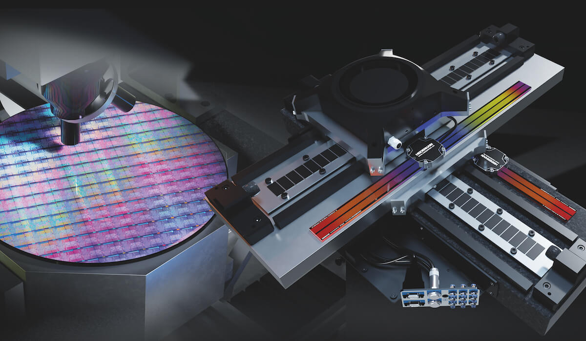
This, of course, requires motion control technologies to keep pace with these requirements for unprecedented, combined speed, accuracy, and precision (Figure 1). Concurrently, nobody wants to see throughput metrics decrease, which creates a constant drive for increased accuracy and precision at high production throughput.
Demands for Increased Precision
An example of one such relatively new manufacturing process is die-to-wafer hybrid bonding, where dies are stacked one on top of each other and interconnected via fine copper interconnects. This enables a previously unachievable density of connections, surpassing the limits of conventional copper bump technologies and considerably minimizing signal delay and attenuation.
However, a higher density leads to tighter tolerances, and thus far more accurate motion control in the bonding process is needed than is the case with conventional alternatives.
Another new development in this segment is fan-out wafer-level packaging (FOWLP) including new more stable substrates. Despite having been invented more than 20 years ago, fan-out package design has garnered substantial interest from today’s market and is currently seen as a worthy alternative to fan-in, particularly over the last five to ten years.
Compared to standard wafer-level packages, FOWLP enables impressive input/output specs within a more compact footprint, while also delivering superior thermal and electrical performance. As the die gradually becomes smaller, fan-out packaging enables the very high interconnect densities that are present on smaller dies.
Unfortunately, the required production process is quite complex. FOWLP requires the reconstitution of the wafer with a die embedded into low-cost materials, which enables high-cost silicon to become more efficient. However, this process is coupled with precise fabrication steps, which slow down production, challenging producers’ cost-of-ownership (CoO). The relationship is clear: the higher the density, the finer the connection pitch, and the higher the placement speed and accuracy requirements.
Balancing Accuracy and Throughput
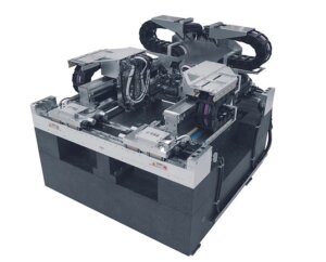
Tool selection in the semiconductor industry is predominantly driven by CoO. For back-end applications, CoO is typically defined as a combination of cost per bond and yield. Both metrics are directly linked to positioning accuracy and throughput of the motion system used in the chip integration process (Figure 2). There is no tolerance for yield loss of finished ICs, therefore the reliability of the packaging integration process needs to be extremely high.
One can have all the bandwidth, AI, and optics in the world, but none of this matters when a semiconductor tool cannot achieve nanometer-level precision without compromising production throughput. When the goal is to take high-precision measurements as quickly as possible, the maximum speed of a motion system’s axis must be delivered with minimum settling time or measurement on the fly. There are usually multiple tradeoffs present and thus, by design, conventional motion system architectures are optimized either for high positioning accuracy or for high throughput.
To achieve the coveted combination of speed, accuracy, and stability, more advanced processes and motion technologies are needed, i.e., encoders for capturing position and speed, as well as motion control systems for high-precision movement of tools and components.

Motion Control Systems Set to Assume a Leading Role
Advances such as FOWLP introduce multiple variables into the production process, creating a higher probability of imperfections in the final product. Furthermore, this approach also requires extreme speed and consistent pinpoint accuracy for efficient, profitable semiconductor manufacturing.
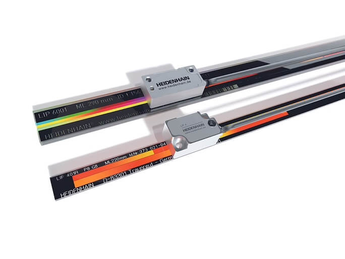
There are two core technologies that are proving decisive in achieving success with this new production strategy. The first key element of this approach is the very compact HEIDENHAIN LIP 6000 encoder that delivers an impressive signal stability of 0.4 nanometers at 1 MHz, enabling the motion system to achieve millisecond-level seek and settle times. Secondly, ETEL controls utilize algorithms to calculate the optimal path performance for inspection similar to those that are used to help race car drivers follow the most optimum racing line.
ETEL’s TELICA motion system is an advanced high dynamic motion system platform dedicated to precision backend semiconductor processes that enables the process to achieve sub-micron placement accuracy required for advanced, next-generation packages. This high level of accuracy is maintained over a work area of up to (870 x 800 mm), which concurrently enables very high-duty cycles and throughput.
TELICA is now introducing an entirely new approach comprising a secondary metrology loop at the process plane level. This drastically reduces Abbé errors as well as the relative positioning mismatch between the process tool and substrate. Multi-dimensional encoders ensure that the placement accuracy level is achieved in up to six degrees of freedom, while water-cooled ‘iron core’ motors enable extreme yet reliable duty cycles.
The metrology frame concept also reduces any vibration feedback loop within the system that acts on the tool point, thus minimizing disturbance in the desired placement, process, or inspection steps. As high throughput target placement capabilities in the sub-50 nm realm emerge for heterogeneous chiplet integration strategies, especially when future hybrid bonding processes as considered, a fully integrated motion system including an active isolation platform, multi-axis stage, advanced motion control electronics, and algorithm architecture becomes necessary.
Conclusion
The semiconductor industry’s relentless drive towards 3D structures and emerging advanced packaging techniques to drive “More than Moore’s Law” objectives require increasingly more complex, precise, and reliable production processes.
These new developments in the motion control space are permitting manufacturers to meet and exceed these strict precision requirements, whilst still maintaining a more than satisfactory throughput, and cost of ownership. The semiconductor industry will continue to innovate beyond the apparent physical limits of silicon transistor production and manufacture devices at the system level that deliver superior performance coupled with power efficiency, all within a standard package footprint or perhaps extending module package sizes.
Power and heat dissipation from these complex multi-chip systems will continue to challenge the industry as compute demand continues to scale in high-speed AI applications.
This article first appeared in the 2024 3D InCites Yearbook. Read the issue here.