
As the semiconductor packaging technology evolves in the “More than Moore” era, many advanced processes have presented challenges in manufacturing. Often, challenges in precision die bonding, for example, have led to trade-offs in yield, throughput, and ultimately manufacturing cost. Precision alignment has become one of the key capabilities for several advanced technologies for heterogeneous integration, such as 2.5D/3D, optical assembly, etc.
For advanced packaging, over the years, as the package pitches continuously decrease for high-density designs, die bond alignment at finer pitches, such as 10µm or below, has become a key challenge area. For flip-chip die, for example, there is a cost tradeoff with high accuracy on most bonding equipment —- the tighter the pitch, the slower the die bond alignment process.
Limitations on the die alignment precision often can impose limits on the device integration density that can be achieved using 3D stacking. High-density fan-out is another process that requires high-precision die bonding. Once the requirement for die alignment precision goes below 1μm, challenges in yield and throughput become even more severe. For hybrid bonding, for example, the alignment precision of the equipment can be a limiting factor for the interconnect pitch, thereby limiting the realization of the design requirements in certain situations. The emergence of chiplets presents even greater challenges for volume manufacturing.
High precision alignment is also a critical capability for transceivers, fiber optics, MEMS, LiDAR, LED, optical imaging, and others. These important applications demand high precision alignment and high throughput simultaneously, further pushing the capacity limit of the equipment. For optical assembly, for example, lens attach, transmitter placement, receiver position, bond line thickness (BLT), etc. are all critical parameters for process yield and product performance.
Machine learning and artificial intelligence (ML/AI) can be very effective tools to help address these challenges.
Machine Learning is focused on finding patterns in data and using those patterns to make predictions. ML/AI can have many important applications in semiconductor packaging and electronics manufacturing. These range from supply chain management, new product introduction (NPI), production planning, traceability, to predictive maintenance, productivity improvement, and process improvement, yield improvement, among others.
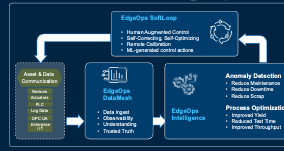
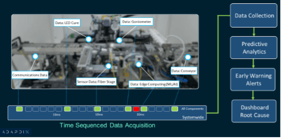
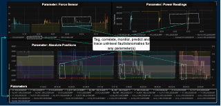
One example is an ML/AI platform that utilizes real-time machine data and operational data (such as actual placement positions, cycle time, etc.) to develop ML models right there at the machine (i.e. at the “edge”). Easy interfacing with the machine data sources (such as existing sensors, actuators, PLC, log data, etc.) via appropriate communication protocols, make available a large body of real-time data (such as acceleration, rotation, conveyor speed, gripper position, bonding head motion, epoxy dispense pressure, and other real-time parameters of various machine parts),. which are important for machine and process performance. Real-time data ingestion and multi-variable data processing, in combination with data transformation, stitching, and filtration, provides a robust foundation for mass data virtualization for building ML models (Figure 1).

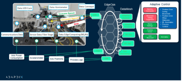
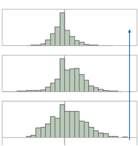
The platform collects data in milliseconds and builds ML models in days and weeks, in an actual manufacturing environment without interrupting production. The ML models, through continuous refinement in real-time, are used for predictive maintenance (by anomaly detection) (Figure 2) and more importantly, for adaptive control of the machine itself (Figure 3). These capabilities have been leveraged by several large global enterprises for semiconductor fabs, advanced packaging, fiber optics for transceivers, precision placement for SMT, etc. Significant improvements have been achieved to improve the alignment accuracy and process yield while reducing cycle time and machine downtime (Figure 4).
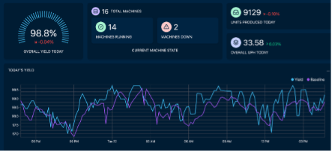
In the meantime, visualization (Figure 5) and traceability (Figure 6) can be realized from the site/line-level all the way down to machine sensor level, with granularities unimaginable before, offering unprecedented insights and intelligence for optimization and continuous improvements. This solution (or “hybrid” as required) also ensures data security and low latency. As the platform is machine agnostic, it can be deployed onto various machines on the line across the factory. This is particularly powerful as upstream and downstream machines can now “collaborate” for overall synchronous optimization.
Through various use cases, it has been demonstrated that the ML/AI platform at the edge can be utilized to significantly improve the machine performance as well as yield and throughput for challenging processes, particularly for precision alignment, for semiconductor fab, advanced packaging, optical assembly, and others. Certainly, it can also be used for diagnosing complex, multi-variable process problems, as well as for reducing test time by leveraging the data from the various stations of the entire production line.
For further information about ML/AI in semiconductor packaging and electronics manufacturing, please contact Dr. Dongkai Shannguan at Adapdix.