Fan out (FO) packaging is one of the key growth segments in advanced packaging, with high adoption rates and strong technology advantages offering a strong pathway moving forward to support industry roadmaps. The nature of reconstituted substrates is now enabling fan-out panel-level packaging. Fan out packaging is no longer limited to the silicon wafer format, opening up a whole new range of possibilities. OEMs are aggressively driving their contract manufacturers to utilize these new substrate sizes and packaging processes to leverage cost savings. Qualifying power management ICs (PMICs) and developing the next generation of chiplet packages are interesting challenges that lay ahead now that high performance, fab-compatible (full SECS/GEM and OHT integration, etc.) panel solutions are commercially available.
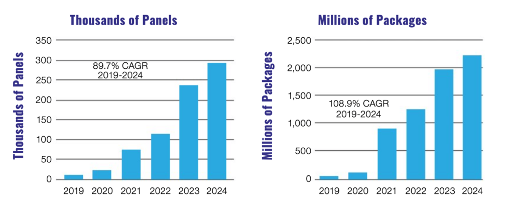
The first developments for panel-level equipment and process solutions were undertaken by the supply chain five years ago, and since that time the first R&D and pilot lines were established. These lines evolved into pilot production in 2020, and in 2021 we will see early adopters finally move into high volume manufacturing with a wider range of products. As reported by Yole Développement, leading companies like Samsung, Nepes, and Powertech International (PTI) have publicly announced their readiness. Others like ASE Group, Amkor Technology, and newcomers like ESWIN are coming to the end of their final technology qualifications as 2020 closes and are ready to take the next big step by including panel packaging into their product offerings. All this can be considered as the first wave of panel-level packaging.
Next-generation developments in systems in package (SiP) or solutions for AI and high-performance computing (HPC) applications will also then push the industry towards very large package bodies. This second wave will also require panel-level packaging (PLP) technologies as wafer dimensions and shape will severely limit the overall substrate utilization and be detrimental to the overall cost of ownership. Of course, technical process performance, handling capabilities, and semiconductor-like quality must be proven. Missing industry norms and standardization were an issue in bringing the technology to market over the last few years but finally, we at least see consolidated panel sizes for 600x600mm and 510x515mm in the industry (Figure 1).
Market Outlook
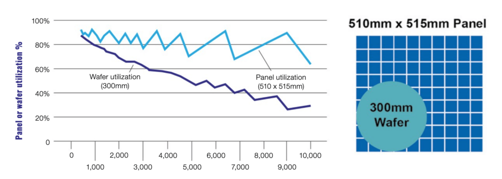
Establishing PLP manufacturing lines does require investment in dedicated panel equipment for temporary bonding, pick-and-place, molding, grinding/polishing, sputtering, resist lamination, lithography, electroplating, and etching. Utilizing 300mm equipment might then be reasonable for back-end-of-line (BEOL) processes such as testing and dicing. Nevertheless, PLP certainly offers the potential for lower cost of ownership due to the larger substrate area and better economical manufacturing of bigger packages because of better material utilization. Many analysts have looked at the merits of moving from wafer to PLP packaging in more detail. It is certainly clear that with a bigger size of substrate the substrate cost portion per package should see a significant reduction due to economies of scale.
Within a typical FO manufacturing process, the redistribution layer (RDL) cost is considered one of the key contributors at around 40%. The largest costs for the RDL itself come from material costs like photo dielectrics and plated Cu, followed by Capex costs for lithography and metallization equipment. In moving from wafer to panel, the contribution of material costs is expected to stay at a similar level, so cost reductions will be sought in equipment that simply processes larger substrates with more packages at the same time. Multiplying the output by a factor of three or more, but still achieving the same level of process performance on 500mm panels as on 300mm wafers, is the biggest argument for PLP. Rectangular substrates are also preferred over round when it comes to material utilization — especially with bigger packages as illustrated in Figure 2.
at the panel level get bigger with die size ( As presented by Intel at IMAPS 2020)
Process technologies like lithography, seed layer deposition, and electrolytic plating play a key role in enabling cost-effective, reliable high-volume manufacturing on large substrates. After a long period of investment in hardware and process developments, the equipment industry is now able to provide tailored equipment solutions.
Sophisticated technologies might continue to drive device technology forward at the wafer level, but the baseline expectation is that performance at panel level will keep up to match whatever is achieved on a wafer-scale.
Fan-out Panel-level Package Solutions are Here
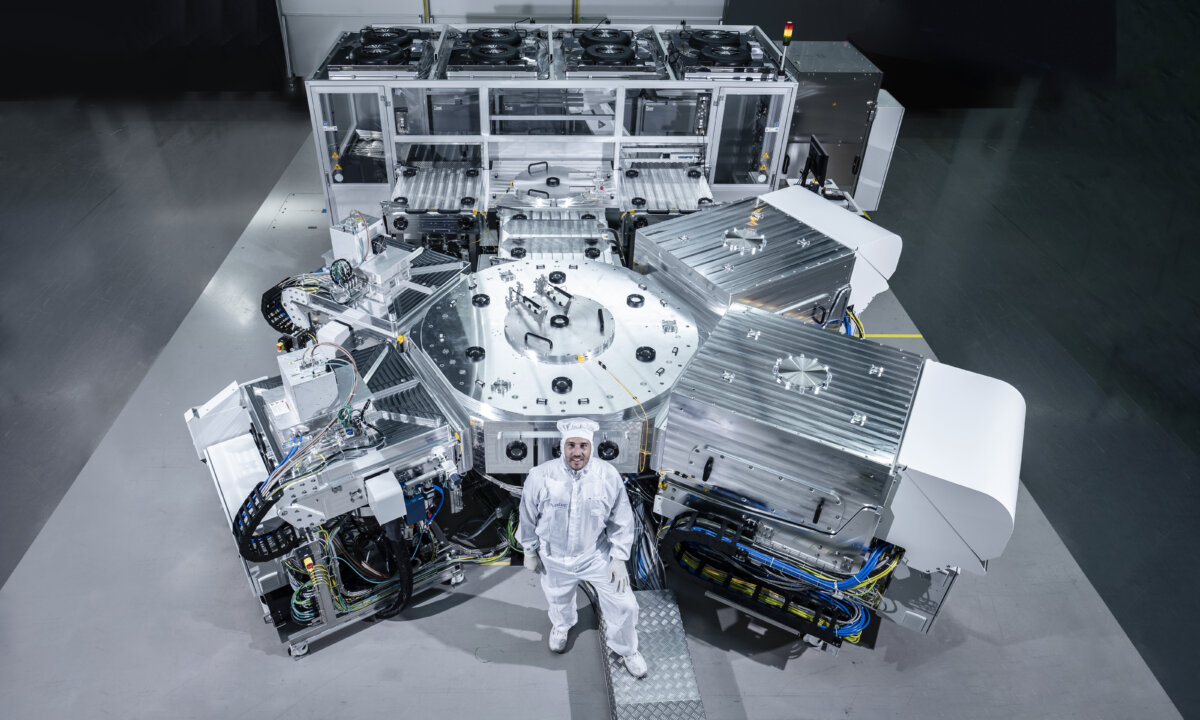
The feature photo above shows an example of a commercially available SEMI compatible cluster tool designed for panel sizes up to 650x650mm.
We believe It’s going to be an exciting time for the advanced packaging industry and panel processing technology as capacities ramp in the years to come, but if you don’t believe us why not listen to what the industry experts say. The situation was well summarized by Boris Hsieh, CEO of PTI inc. in a recent interview with Digitimes:
“In terms of advanced packaging technology, TSMC now offers the largest InFO capacity in the world and Samsung Electronics also has its own advanced packaging solutions, but PTI now focuses on FOPLP technology. We are continuing negotiations with potential clients over the FOPLP backend services.
If InFO and FOPLP are both suitable for packaging some types of ICs, the latter can offer more-cost-effective production as panels can be cut into subpanels that will involve simplified processes and competitive cost structures to help clients save production cost. And we are targeting leading vendors of networking chips as potential clients for our FOPLP services, and it will not be impossible for us to serve even vendors of GPUs and handset APs in the future.”

Editor’s Note: To learn more about Evatec’s work in FOPLP, read the companion process technology post, What Does Panel-level Packaging Mean for Seed Layer Deposition? here. These articles first appeared in the 2021 Yearbook. Find it here.
About the Authors
 Ralph Zoberbier, lead author of Fan-Out Panel-Level Packaging Takes Off is head of the advanced packaging business unit at Evatec. He has more than 20 years of experience in the semiconductor equipment business, with roles in engineering, product management, and global business and sales management. In addition to thin-film technology, his technical expertise covers areas including lithography and ECD for both wafer and panel level applications.
 Roland Rettenmeier, co-author of Fan-Out Panel-Level Packaging Takes Off is Senior Product Marketing Manager at Evatec, where he focuses on business development for emerging applications like EMI shielding and advanced IC substrate processing. Rettenmeier is a Mechanical Engineer and completed his executive MBA studies in Austria in 2005. He has experience in electronics and semiconductor manufacturing, managing projects in China, Switzerland, and Austria since 2001.
 Allan Jaunzens, a co-author of Fan-Out Panel-Level Packaging Takes Off, is the head of marketing and communications at Evatec. Allan trained as a materials scientist gaining his first experience in the thin-film technology industry as an R&D engineer 30 years ago. Since that time, he has remained in the field holding numerous positions in international sales and service management before joining Evatec in 2006.