Seed layer deposition is one of the most critical process steps in manufacturing vertical and horizontal interconnects. At the panel level, seed layer deposition must deliver high-performance degas, etch, and sputter deposition processes as well managed substrate temperature throughout the whole process to ensure low contact resistance (Rc) and excellent adhesion of the seed layers prior to downstream processing. (litho, electroplating, etc.).
Step 1: Repeatable and reliable outgassing of organic substrates
Degassing is an important first step in ensuring good bond strength for the seed layer. Industry solutions so far have included both atmospheric and vacuum approaches. Diffusion of volatile components from the bulk material to the surface is driven by temperature and time.
Desorption is driven by the concentration gradient which is the same whether desorption takes place under vacuum or in atmosphere. However, the advantage in atmosphere is that the concentration gradient can always be kept high if a laminar flow of inert gas is applied, while under vacuum, the degassing of the volatile components has to take place by less efficient molecular diffusion. So far, it looks like atmospheric technology where a batch of substrates are simultaneously degassed in multiple heated slots with nitrogen laminar flow will be the winner for organic substrates (e.g. AMC, ABF, PID, PI, etc.).
Features favoring atmospheric degas technology include fast and precise temperature control of substrates (conductive heating), emissivity independent temperature control (no overheating and no local hot spots), and transport of volatile compounds away from the substrates (no re-contamination)
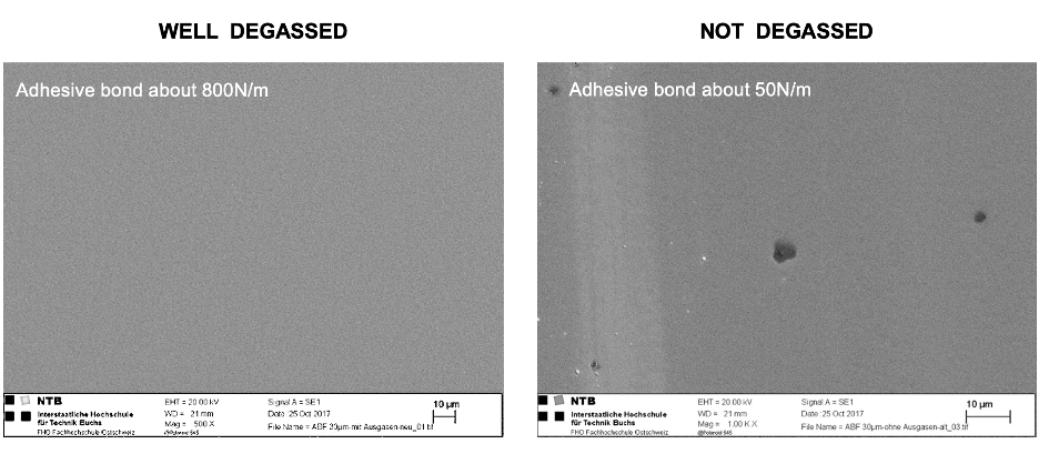
SEM images in Figure 1 illustrates film quality on ABF GY50 substrates with and without prior degassing. Without proper degassing, the films can end up with defects such as voids or holes. In peel testing according to IPC standards, adhesive bond strength was measured at 800N/m for well-degassed substrates but only 50N/m for equivalent processes omitting the degas step.
Step 2: Etching processes — perfectly tuned for large-area panel processing
Removing native oxides and preparing the substrates’ interface are the major reasons for etching in advanced packaging. Low Rc and superior adhesion of the sputtered seed layer are the results.
Key requirements for high process repeatability and yield are high etch uniformity over large areas with low edge exclusion and particle avoidance. Substrate damage must be avoided by controlling plasma densities and ion bombardment, while etch powers/rates also need to be managed to remain within thermal budget.
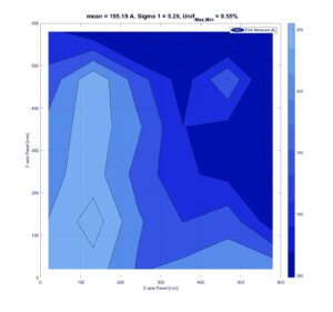
Etch uniformity results on a panel size of 600m x 600m using a capacitively coupled plasma (CCP) source are shown in Figure 2. The achievable uniformities of <10% fall within the specifications demanded by process developers and processing with a static panel addresses the key concerns of reducing the risk of particle generation.
Some process technologies such as laser via descum or forming vertical interconnects will also require combinations of physical and chemical etch (CHF3, C3F8, CF4, O2, N2+H2, Ar+H2, etc.)
Step 3: Sputter deposition – Superior seed layer adhesion and uniformity
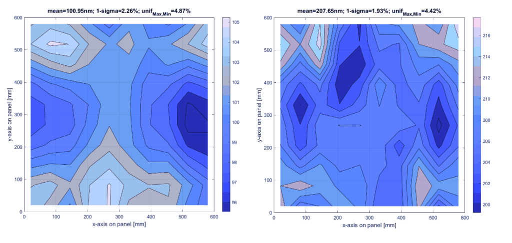
Just like for the etch process, key performance specifications for overall process yield include high deposition uniformity with low edge exclusion and avoidance of particles. Deposition uniformity results for the required Ti and Cu layers are shown for panel sizes of 600mm x 600mm in Figure 3.
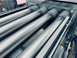
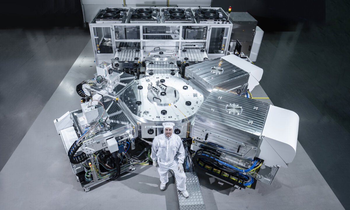
In this case, rotating target sputter technology (Figure 4) also enables processing static panels to reduce the risk of particle contamination while still achieving the required deposition uniformities.

Editor’s Note Wondering more about the fan-out panel-level packaging market? Read the companion Executive Viewpoint here. Both appeared in the 2020 Yearbook. Find it here.
About the Authors
 Ralph Zoberbier, lead author of Fan-Out Panel-Level Packaging Takes Off is head of the advanced packaging business unit at Evatec. He has more than 20 years of experience in the semiconductor equipment business, with roles in engineering, product management, and global business and sales management. In addition to thin-film technology, his technical expertise covers areas including lithography and ECD for both wafer and panel level applications.
 Roland Rettenmeier, co-author of Fan-Out Panel-Level Packaging Takes Off is Senior Product Marketing Manager at Evatec, where he focuses on business development for emerging applications like EMI shielding and advanced IC substrate processing. Rettenmeier is a Mechanical Engineer and completed his executive MBA studies in Austria in 2005. He has experience in electronics and semiconductor manufacturing, managing projects in China, Switzerland, and Austria since 2001.
 Allan Jaunzens, a co-author of Fan-Out Panel-Level Packaging Takes Off, is the head of marketing and communications at Evatec. Allan trained as a materials scientist gaining his first experience in the thin-film technology industry as an R&D engineer 30 years ago. Since that time, he has remained in the field holding numerous positions in international sales and service management before joining Evatec in 2006.