
Sometimes, in the face of adversity, great things can be accomplished. In this case, the adversity was the COVID-19 crisis, and the great things accomplished were the goals of the Panel Level Packaging Consortium 2.0.
In a recent article published by Fraunhofer IZM, Dr. Tanya Braun, group leader of the Panel Level Packaging Consortium 2.0 reported on the progress the 17 international partners achieved in its first year. This is a continuation of the work begun in 2016 to develop the fundamental processes needed to take panel-level packaging (PLP) from concept to industrial scale, high volume production.
Braun explains that for its first run (PLC1), the group focused on the entire PLP process chain, from assembly, molding, wiring and cost modeling to standardization. With the launch of the Panel Level Packaging Consortium 2.0 (PLC2) “the focus shifted to die placement and embedding technology for ultra-fine-line wiring down to 2µm lines and space, with the potential to move to 1µm.”
Because of the pandemic lockdowns, access to lab work was restricted. To adjust, the group extended the work plan by four months. All the meetings were conducted virtually with two sessions to accommodate time zones. Still, despite these hurdles, Braun reports that the group made great progress – from new panel-level packaging equipment installs, to significant funding.
From a technology perspective, they made progress finding root causes to warpage and die shift in large re-constituted panels. This will make it easier to control parameters for fine-line/space redistribution layers (RDL), “making the most of the advantages of both wafer and panel-level technologies and paving the way for an entirely new process chain with new equipment and materials.”
The partner companies include Ajinomoto Fine-Techno Co (AFT), Amkor Technology (Amkor), ASM Pacific Technology Ltd., AT&S Austria Technologie & Systemtechnik AG, Atotech, BASF, Corning Research & Development Corporation, Dupont, Evatec AG, FUJIFILM Electronic Materials U.S.A., Intel Corporation, Meltex Inc., Nagase ChemteX Corporation, RENA Technologies GmbH, Schmoll Maschinen, Showa Denko Materials Co. Ltd (former Hitachi Chemical Company, Ltd), and Semsysco GmbH.
Among them, AFT, Amkor, Atotech, and Evatec are 3D InCites community members. I caught up with Habib Hichri, AFT; Jose Silva, Amkor; and Ralph Zorberbier, Evatec; to learn more about their experiences. Each had a different and interesting role to play as an OSAT (Amkor), a material supplier (AFT), and an equipment supplier (Evatec). All these companies participated in PLC1 and have continued into PLC2. Here are some highlights from their perspectives:
What Is Your Company’s Role in Panel Level Packaging Consortium 2.0?

Jose Silva – Amkor Technology: Initially, Amkor engaged in the PLC1 as Nanium, and then after the acquisition by Amkor, we renewed our membership in PLC2 as Amkor. While we don’t have any obligations to perform work or disclose information, we play a role in influencing the direction of the investigations and have access to the developments. We have also been participating in the revision board and the information is being shared with Amkor Global R&D Center in Korea (K5). Additionally, we have an agreement to use their equipment for our own activities, which is what we did while we waited for ours to be up and running. (Note that all activities performed in their equipment were covered by a contract and were not performed as part of the consortia.)

Habib Hichri – Ajinomoto: AFT has collaborated previously with the IZM team using our ABF materials in their wafer-level packaging process development. Our film-format ABF materials are used for RDL fabrication. For example, our nanofiller ABF allows resolution for fine via using laser or etch patterning processes with smooth sidewall angles. In parallel, we also provided photo-dielectric materials for fine via fabrication using photolithography technology (mask-based or maskless).

Ralph Zorberbier – Evatec: Evatec joined the first round of the PLC in 2016 as we recognized panel-level packaging would be a key market development back in 2015. We joined as full members to ensure the most effective participation. Our key contribution to PLC2 is in the field of thin-film deposition, RIE/DRIE, and plasma descum for FO PLP and next-generation IC substrate applications and technologies.
Why did your company choose to participate in PLC 2.0?
Jose Silva – Amkor: Fraunhofer IZM has excellent capabilities and know-how. We have cooperated in different projects with them before. We joined PLC1 and PLC2 because we are interested in being informed about the developments of Fraunhofer IZM’s PLP technology. We wanted to be involved in PLP development, participate in the technical discussions, and assess a possible move into this market. We also wanted to leverage the opportunity to engage with industry leaders, mainly in equipment and materials.
Habib Hichri – Ajinomoto: Fraunhofer IZM is highly regarded and well-respected in the semiconductor advanced packaging industry. We appreciated the opportunity to become a member of PLC2 because it provides us with valuable real processing data that helps us respond to our customers’ questions and concerns. In addition, it is beneficial to work closely with other materials and equipment suppliers to provide panel-level packaging solutions.
Ralph Zorberbier – Evatec: The IZM-initiated consortia is the industry’s most effective and industry-focused consortia that bring key technology leaders from the supply chain together with end-users. This fosters close collaboration and networking across the equipment and material supply chain and enables open discussions and alignments on key applications and market requirements on real product examples.
In such a new field, standardization and alignment across the full manufacturing areas including package design and material selection are crucial to successfully bring this new technology to the market. It requires know-how and an experience exchange which is only possible in such an open environment. From the very beginning, IZM managed to motivate leading companies in all relevant areas to join.

What technology challenges did your company help address?
Jose Silva – Amkor: For PLC1, we helped with the development of the cost model. As the work itself is realized by Fraunhofer, beyond our role on the revision board, we did not perform any work in year one of PLC2.
Habib Hichri – Ajinomoto: The trend for high IO is to achieve <10µm vias and 2/2µm line/space RDL at the panel level. We participated in this consortium to provide solutions to these fine features using our ABF materials. We provided nanofiller ABF that can reliably achieve the needed fine resolution for both L/S and via. Additionally, we provided photo-dielectric materials for PLP for fine via fabrication using photolithography technology (mask-based or maskless).
We also helped overcome the challenge with local and global warpage that is known to impact patterning processes and eventually yield. Our molding materials contain additives that relax mold film during curing and reduce the stress that contributes to the warpage.
Ralph Zorberbier – Evatec: Our key contribution was in the area of RDL and vertical interconnect fabrication. We are focused on the development of an RIE/DRIE process on a panel scale. Highly uniform seed layer deposition at the lowest contact resistance on large-scale substrates is the biggest challenge, especially when you need to consider substrates with high organic load and a high emissivity mix. In addition, micro via formation in ABF-like materials requires new manufacturing methods to meet the industry requirements from a technical but also cost perspective.
What progress did you make with your part of the project?
Habib Hichri – Ajinomoto: IZM demonstrated impressive results using our nanofiller ABF for reliable fine via and RDL on PLP. Our latest photo-dielectric materials KT7 series showed the capability of fine via of 2µm in 2µm thick material and good b-HAST reliability for 1.5/1.5µm L/S at 3.3V. Lastly, our molding materials in both film and liquid form were selected by IZM among other competitors’ materials for their packaging application given their molding properties such as warpage, flow mark, and reliability.
Ralph Zorberbier – Evatec: Driven by the PLC program, we were able to accelerate the deployment of our know-how from FO WLP to PLP. We could adjust the seed layer process to match perfectly with up and downstream processes to ensure a seamless process integration in the manufacturing process chain. Another major supporting factor was the integration and build-up of know-how in new materials targeted to be used for panel-level packaging. Based on the collaboration within the consortium, Evatec could develop and further optimize a DRIE process to manufacture small vertical interconnects using state-of-the-art ABF dielectric materials. This new process is ready to meet the requirements of next-generation substrate build-up technologies in terms of technical capabilities, reliability, and cost.
Functioning During COVID-19
Prior to the pandemic, the PLC met in person and members also had the opportunity to tour the fabrication line and address any technical issues that may require intervention, explained Hichri.
Since the pandemic, all PLC2 progress meetings were conducted via video-conferencing, noted Silva.
Zorberbier added that a key element to completing the research was “close communication coupled with ‘FedEx flow sampling’.”
“We continue to communicate via emails, and we can request conference calls at any time, when necessary,” said Hichri. “The team at IZM are supportive and committed to achieving the agreed-upon technical goals and are responsive in providing feedback. We are content with our membership with the PLC consortium, and we are committed to continuing working with IZM for future development projects.”
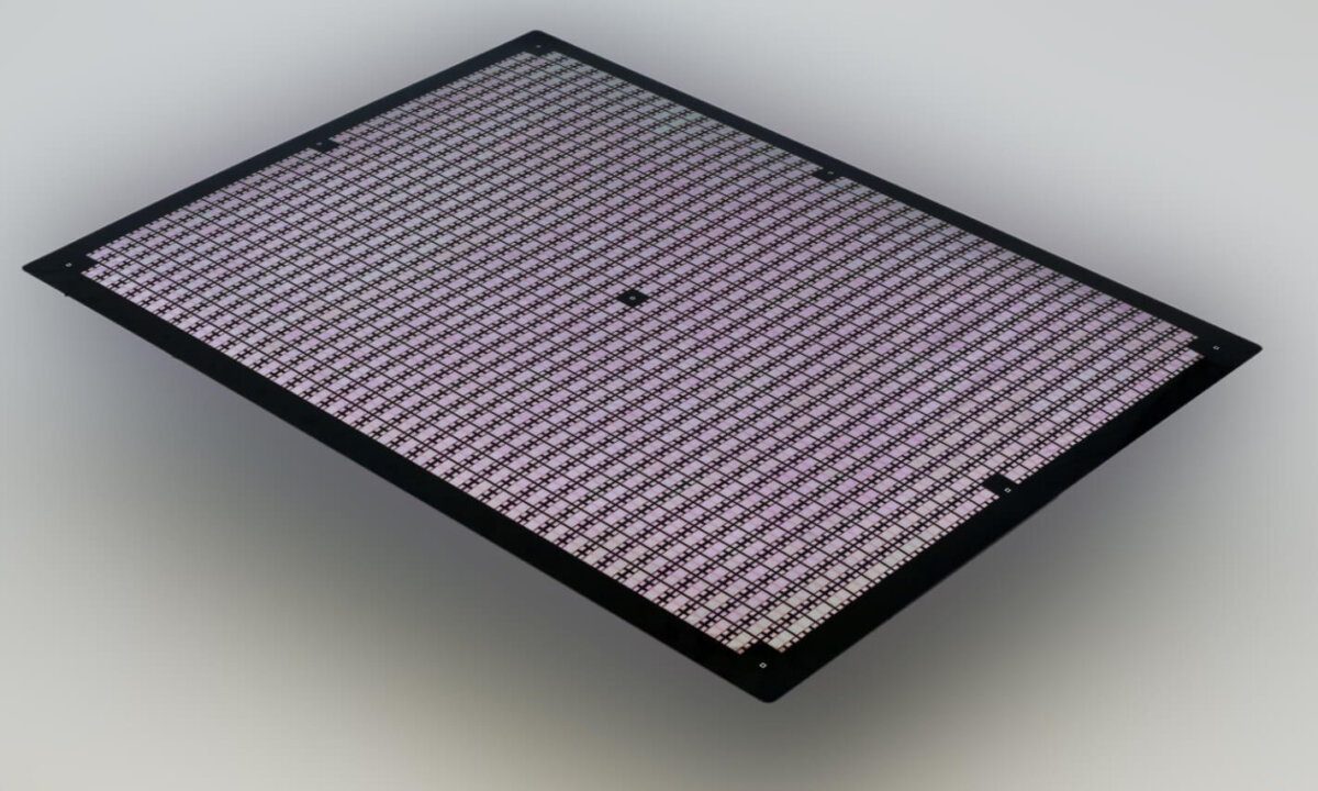
Feature image above: First results of PLC 2.0: Fully populated panel with embedded chips. Copyright – Fraunhofer IZM

