
Continuing our look at presentations at the 2022 ECTC, who better to examine the question “Panel Level Packaging – Where are the Technology Limits?” than Tanja Braun and the group at IZM Fraunhofer who have become experts in this processing area over the last several years? Although they do not come up with all the answers you might want to see, they give a great update on the status of this complex technology.
Fan-out wafer level packaging (FOWLP) and fan-out panel level packaging (FOPLP) are two of the dominating trends in microelectronics packaging. But IZM reports that for FOPLP, it is still not fully clear if the same performance can be achieved at the wafer level since processing on large panel sizes results in higher challenges in process control, accuracy, and consistency.
Recently, FO-PLP has been introduced to high-volume manufacturing. Nepes, Samsung, Powertech, Unimicron, ASE, and Eswin have either started FOPLP in volume production or are qualifying PLP processes and will be ready to start soon. Although new materials and equipment have been introduced for FOPLP the technical and physical limits are still unclear.
The main driver for moving to panel-level packaging is of course lowering the packaging cost. On panels, more packages can be processed in parallel and there is a much better area utilization than for round wafers. This paper describes current technology developments at IZM to access the limits of panel-level packaging technology. Warpage, die shift and fine line capabilities are examined in detail.
For large panel processing, an adaptive patterning approach (think DECA) might be needed to achieve a high yield. Here, the combination of an intelligent assembly strategy for high speed and sufficient accuracy capabilities to measure each die position, and a maskless lithography process adapting the redistribution layer (RDL) to each die position, may lead to a cost-effective high yield process.
In addition, a clear trend toward finer lines and spaces as well as smaller via diameters are also demanded for large panel RDL processes. Process developments towards 2μm L/S and via shrinking on 610 x 457 mm² panels are detailed.
At IZM a “chips first”, face-down approach has been selected (Figure 1).
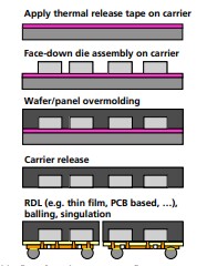
The chip-first face-down process starts with die assembly to an intermediate carrier followed by overmolding and debonding of the molded panel from the carrier. The redistribution layer is then applied to the reconfigured molded panel. For the redistribution layer (RDL) two different approaches have been successfully evaluated on the panel level. In the “thin film approach” (similar to what is typically done on the wafer level) photosensitive polymers are applied as dielectric layers and no further chip preparation is required. Using large panels dry film materials are preferred. Via formation to contact the die is done by laser drilling. Process challenges include (a) warpage, (b) die shift, (c) RDL on KGD (failure in RDL will cause loss of the die)
Impact of Warpage on Panel Level Packaging
For the reconfigured panel, manufacturing dies are placed at room temperature on the carrier with attached thermal release tape. During molding and the curing of the embedded mold compound (EMC), the dies are fixed in the EMC matrix. During cross-linking of the EMC the material shrinks, leading to a change in the volume of the molded panel. This leads to the above-mentioned warpage and die-shift challenges.
Warpage is also mainly based on the coefficient of thermal expansion (CTE) differences of the carrier, EMC, and the embedded die and the chemical shrinkage of epoxy mold as described above for the die shift. The goal is not to minimize the warpage at a certain process step but to keep it controlled through the entire process to guarantee reliable processing.
Die Shift & Compensation
During assembly first, a defined number of fiducial dies are placed creating the reference coordinate system for all other placement steps. The fiducial dies also allow the position measurement after assembly and molding and debonding from the carrier. The final die position in the reconfigured panel is a key factor for the overall process reliability and resulting yield. They found that die shift increases with decreasing overmold thickness and increasing Si density.
An approach to solving this is to adapt the RDL layout to the real die position. The residual die shift error after mold compensation was digitally mitigated by adapting the RDL layout to match actual die positions. This would be similar to what Deca proposes for its technology.

Redistribution Layer
Challenges for the RDL are identified as three-fold. (1) the availability of a maskless direct imaging (DI) tool with high throughput, sufficient depth-of-focus, and PCB/PLP compatibility; (2) the availability of suitable resist material including application methods for panel formats; (3) the data processing for 600 mm² format with 2μm L/S resolution.
Specialized companies doing spin-coating on large panel formats report that upscale challenges are non-trivial, and the large machine footprint makes it not an industrially relevant process. However, alternative methods include dip-, slit, or spray coating and dry film lamination by hot-roll or vacuum application. IZM focused on spray coating and dry film resists. The latter is quite standard in PCB-related manufacturing and has high industry acceptance due to easy application by hot roll laminators and carbonate-based development. IZM reported using vacuum application and achieved L/S down to 3.5μm (partly 3.0 μm) mainly limited by non-sufficient resist adhesion to the sputtered Cu surface. The thinnest dry film resists available to them were 7μm. The aspect ratio of the developed resist structures exceeds 2:1 and they observed collapsing resist lines.
To proceed to lines and spaces down to 2μm, the IZM team evolved a spray coating process to apply liquid resists onto the full-scaled panel size. They were able to fabricate plated Cu structures on Ajinomoto ABF dielectric after barrier/seed wet etch removal of 2.5 /1.5μm L/S.
They note that tables or chucks of analytical instruments are often constructed for wafer sizes up to 300 mm diameter but quality assurance for panel-level processing requires upscaling of such devices.
When approaching 2μm L/S the data handling also becomes challenging for software coming from the PCB world using Gerber or ODB++ type file formats.
Via Technology
IZM uses UV laser drilling of non-photo, highly filled dielectrics from Ajinomoto ABF with a UV/355nm Schmoll Pico drill. They achieved 8 to 9μm laser vias.
They conclude “…new materials, new equipment, and smart manufacturing will further drive PLP to finer features sizes and higher integration levels on large panels but also increase the yield and therewith also improve cost and environmental aspects”
IFTLE is still waiting to see something like TSMC InFO technology done on a PLP. That will be truly impressive.
For all the latest in Advanced Packaging stay linked to IFTLE……………………………………….


