The semiconductor industry has entered a new era and the role of design including the package has become increasingly important. No longer can the industry count on monolithic integration to achieve the economic gains of the previous era. New packaging solutions are being adopted to achieve the economic advantages that were previously met with silicon scaling. The role of heterogeneous integration, especially chiplets, is pivotal in this new era. In fact, TSMC indicates that the use of chiplets will be one of the most important developments for the next 10 to 20 years.
Drivers for the New Era
In the mid-1960s, Intel’s Gordon Moore observed that by shrinking transistors, it would be possible to double the number of transistors that fit onto an integrated circuit every year (revised to roughly every two years) providing a cost advantage to scaling. With the high cost of monolithic integration, this observation no longer holds true to the same extent it once did. Smart packaging is the new way to extend this observation and the use of chiplets has become key.
What are Chiplets?
A chiplet is a functional circuit block and includes reusable IP blocks. It can be created by partitioning a die into functions and is typically attached to a silicon interposer or organic substrate today, but new options are emerging. TSMC argues that the demand for chiplets is driven by the need for a more cost-effective solution, the reuse of IP, and new test flows. A cost reduction is possible because the die functions, such as I/O control, are split out. These die functions are more difficult to scale, requiring more time and money. Cost reduction is achieved by chip integration. With chips divided into two, the split chips can be stacked to provide a 20 percent cost improvement. Chip partitioning also improves time-to-market. The chiplet is not a new idea, but EDA tool improvements are making new architectures possible.
TSMC
TSMC proposes its bumpless System on Integrated Chip (SoIC™) as one chiplet solution. The SoIC™ is a 3D structure formed by stacking logic, memory or both chip types on an active interposer with TSVs. A chip-on wafer (CoW) process is used and the process can handle <10µm bond pad pitch between chips. The chips, with or without through-silicon vias (TSVs), are bonded onto the wafer containing the active interposers using a hybrid bonding process. The 3D chip with TSV SoIC™ also uses through dielectric via and CoW bond. TSMC reports that the SoIC™ structure with its higher density bonding provides better signal integrity, power integrity, and lower communication latency with greater bandwidth than a conventional 3D IC using TSVs and 40µm pitch micro bumps. Lower insertion loss, important for 5G applications, is reported. Lower parasitics and low IR drop are reported. Finer interconnect pitch is possible and there is less concern with CPI because there are no bumps.1
AMD
AMD’s current chiplet solution uses a laminate substrate. AMD has shipped multiple versions of its server processor using chiplets. Up to eight 8-core processors are tightly coupled together on an organic substrate. The chiplets can be binned and speed-sorted before assembly in the package. At the system level, the multi-die package architecturally acts as if it were a monolithic die.2 AMD’s new architecture allows the chiplets to communicate with each other as well as externally, including power and ground management. This new architecture and future approaches will allow performance improvements that cannot be met with monolithic integration, including power consumption
Intel
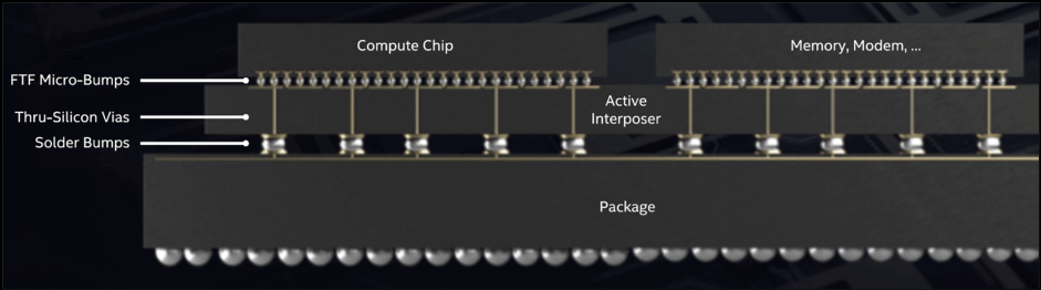
Intel’s latest chiplet solution is called Foveros. It is a 3D integration technology as a form of heterogeneous system integration. Heterogeneous integration is defined as the integration of separately manufactured components into a higher-level assembly or system-in-package (SiP) that, in aggregate, provides enhanced functionality and improved operating characteristics. The technology uses a 3D face-to-face stacking process. In the process, logic dies are bumped and mounted on an active interposer next to memory or die with communication functions such as a modem. The active interposer can contain active parts of the system, such as the platform controller hub (PCH) that manages I/O for the system. The active interposer is mounted on a package substrate with solder bumps (Figure 1). While the first demonstration of the technology used micro bumps, future versions are expected to use hybrid or direct interconnect bonding without a bump.
The Foveros technology will give designers greater flexibility to mix and match IP blocks with various memory and I/O elements into new form factors. Mounting memory on an active interposer removes the bottleneck of memory proximity. Intel is expected to leverage the technology across many product lines.
Conclusions
Chiplets are a heterogeneous integration solution that can move us into the next semiconductor era. While it is technologically possible to continue scaling monolithic die, the economics do not favor this approach. The use of chiplets will become a game-changer in the new era for the companies that can master the design of this new approach.
New players are emerging that will help others participate in the bold new chiplet era. California start-up zGlue offers an online tool, called ChipBuilder, to build chiplets to connect to its smart silicon interposer that allows the use of third-party chiplets. The chiplets, fabricated as wafer-level packages (WLPs), can be connected to an active silicon interposer called Smart Fabric. The company has created a library of more than 250 off-the-shelf chiplets and plans to extend it to more than 1,500 in the near future. In this new era, fortune favors the bold that are able to apply smart packaging as a solution.
![[err-ad-fallback-title]](http://www.3dincites.com/wp-content/plugins/a3-lazy-load/assets/images/lazy_placeholder.gif)
References
1, 2. F. Chen et al., “System on Integrated Chips (SoIC) for 3D Heterogeneous Integration,” Electronic Components and Technology Conference, May 2019, pp. 594-599.
- M. Bhagavat, “Packaging Renaissance with Chiplets,” IMAPS Keynote, IMAPS Conference, October 2019.
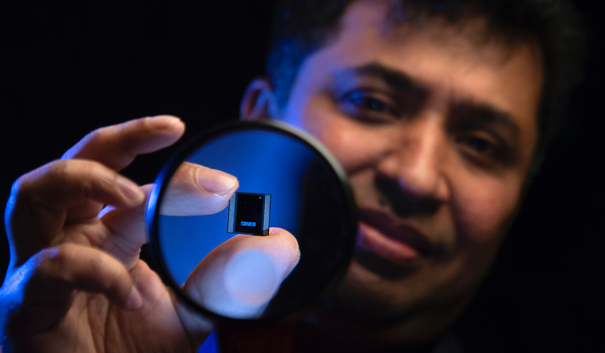
Header Image
Intel Fellow Wilfred Gomes, a member of Intel’s Silicon Engineering Group, holds a processor with the advanced packaging technology called Foveros. It combines unique three-dimensional stacking with a hybrid computing architecture that mixes and matches multiple types of cores for different functions. (Credit: Walden Kirsch/Intel Corporation)
This article first appeared in the 3D InCites Yearbook. Download the issue here.