
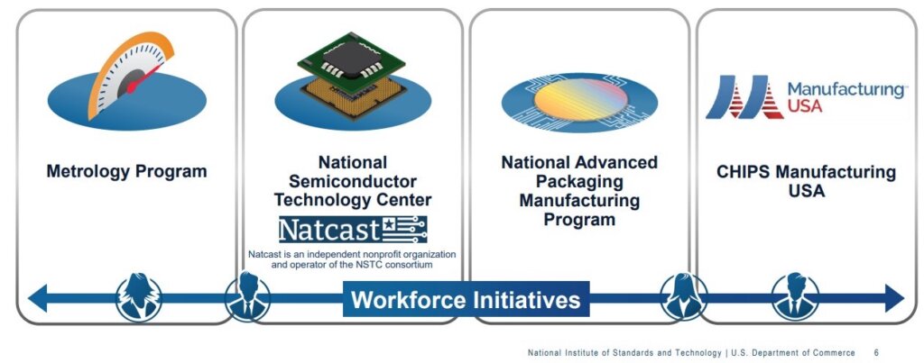
The Creating Helpful Innovations in the Production of Semiconductors (CHIPS) workforce initiatives are shown in Figure 1:
The CHIPS vision for success for the National Advanced Packaging Manufacturing Program (NAPMP) is to establish U.S. leadership in advanced packaging and provide the technology needed for packaging manufacturing in the U.S.
Ex-IBM packaging expert Subu Iyer, currently a Professor at UCLA, is the director of the NAPMP.
The CHIPS NAPMP seeks to enable the development of a robust domestic advanced packaging ecosystem by:
- Establishing an advanced packaging piloting facility (or facilities) that accelerates the transfer of innovations in packaging, equipment, and process development into manufacturing;
- Driving the development of digital tools to reduce the time and cost of advanced packaging engineering; and,
- Establishing and supporting partnerships among industry, academia and training entities, and government to contribute to an advanced packaging workforce.
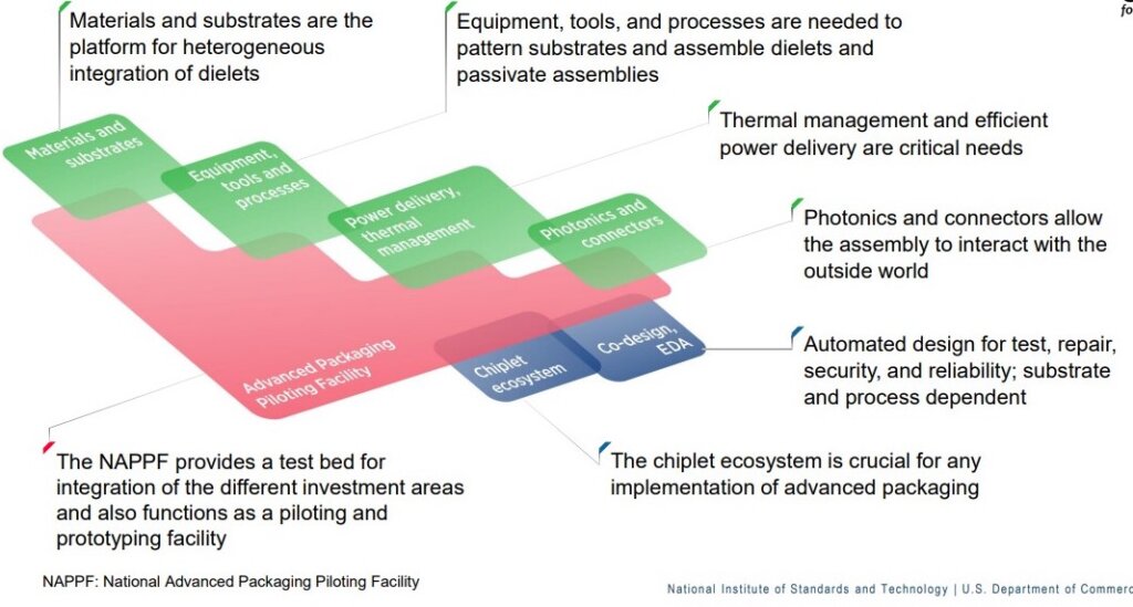
The six priority research investment areas of the CHIPS NAPMP will be:
- Materials and substrates
- Equipment, tools, and processes
- Power delivery and thermal management for advanced packaging assemblies
- Photonics and connectors that communicate with the outside world
- A chiplet ecosystem
- Co-design of multi-chiplet systems with automated tools
In addition, the CHIPS NAPMP seeks to train semiconductor personnel and students to staff domestic manufacturing facilities. The CHIPS NAPMP is chartered to work closely with the CHIPS National Semiconductor Technology Center (NSTC).
NAPMP Substrates and Substrate Materials Program
 A NOFO (notice of funding opportunity) for the first program “Substrates and Substrate Materials” was held on March 1st.
This NOFO seeks applications for research and development activities that will “…establish and accelerate domestic capacity for advanced packaging substrates and substrate materials.”.Through this NOFO, the NAPMP program seeks to:
(1) Accelerate domestic R&D and innovation in advanced packaging materials and substrates;
(2) Translate domestic materials and substrate innovation into U.S. manufacturing,
(3) Support the establishment of a robust, sustainable, domestic capacity for advanced packaging materials and substrate R&D, prototyping, commercialization, and manufacturing
(4) Promote a skilled and diverse pipeline of workers for the domestic advanced packaging industry

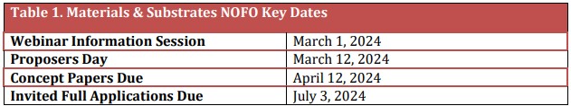
Key program dates are shown below:
The full NOFO can be obtained here.
The overall program scope is shown in Figure 3:
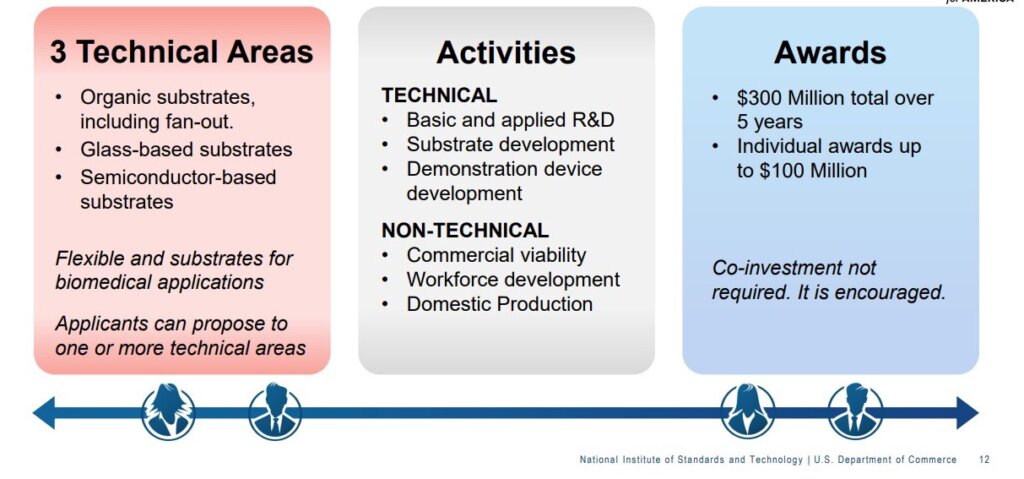
Topics within the program scope:
- Substrate wiring
- Via pitches
- Through substrate vias
- Dual-sided RDL
- Embedded passive & active devices
Specifically listed as NOT within the scope:
- Traditional PCBs
- Interposers
- Small area substrates
IFTLE thinks some tighter definitions will be needed for the community to better understand these items that are NOT considered within the scope of the program…..
For all the latest on Advanced Packaging stay linked to IFTLE………………………….


