
As IFTLE has explained previously, Investments in semiconductors will not succeed without investments in advanced packaging. The CHIPS for America program, agreeing with this premise, has announced that it will support the development of advanced packaging technology in the United States that can be transferred to manufacturing facilities, including recipients of CHIPS IC manufacturing incentives.
The National Advanced Packaging Manufacturing Program (NAPMP) is a $3 billion government program to develop critical advanced packaging technologies and support their transition to U.S. manufacturing entities. (Figure 1).
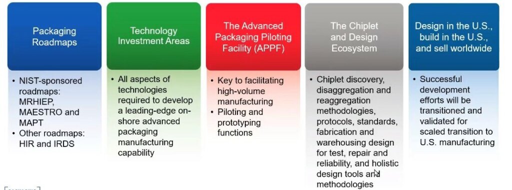
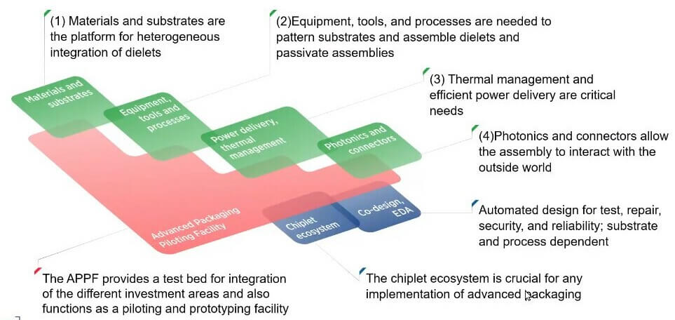
The full vision for the NAPMP has been laid out in this white paper. The program will invest in the following six priority research areas:
- Materials and substrates
- Equipment, tools, and processes
- Power delivery and thermal management for advanced packaging assemblies
- Photonics and connectors that communicate with the outside world
- A chiplet ecosystem
- Co-design of multi-chiplet systems with automated tools

As IFTLE has shared previously Subramanian (Subu) S. Iyer joined the CHIPS for America’s R&D office as the director of the National Advanced Packaging Manufacturing Program (NAPMP). Iyer brings extensive industrial and academic experience and expertise in microelectronics and packaging.
The NAPMP will establish an advanced packaging piloting facility (APPF) (or facilities) “…to help accelerate the transfer of innovations in packaging, equipment, and process development into manufacturing”. Where it all comes together:
Investment areas are expected to connect with activities at the APPF. The group may consider prototyping innovative design ideas from the community.
The APPF is:
- Where successful development efforts will be transitioned and validated for scaled transition to U.S. manufacturing
- A key facility for technology transfer to high-volume manufacturing
The APPF could include:

- Integrated process flows that can reach commercial scale
- Validating new technology specifications, compatibility with other processes, yield, and reliability
- Assessing technologies for scaled transition to U.S. manufacturing
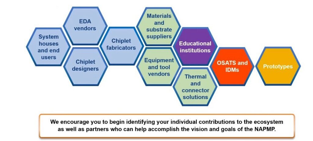
The program will also support the development of digital tools to reduce the time and cost of advanced packaging engineering. The NAPMP is chartered to work closely with the National Semiconductor Technology Center (NSTC), the semiconductor-related Manufacturing USA Institutes, the CHIPS Metrology Program, and U.S. industry and academia.
The NAPMP expects to release its first funding opportunity (expected to be in the materials and substrates area) in early 2024.
Materials and Substrates
According to NAPMP publications, “The key requirements of new substrates include multiple levels of fine wiring and via pitches, low warpage, large area, and the ability to integrate active and passive components.”
- Materials and substrates are the platform on which advanced packaging is built
- These substrates or interconnect fabrics (IF) may be based on silicon, glass, or organic materials and can include fan-out wafer-level processes
- The IF needs to
- be compatible with advanced and legacy nodes and different semiconductor material systems
- have integrable active and passive components
- be compatible with either mass reflow, thermal compression bonding, or hybrid bonding
- Meet environmental and sustainability goals
For all the latest in Advanced Packaging stay linked to IFTLE………………………………

