
This week, we finish our look at papers presented during the IMAPS CHIPCon Conference held in July, 2023, where we focus on North American advanced packaging and new ABF materials. We also applaud the appointment of Dr. Suby Iyer to head up NAPMP, and Dev Palmer’s promotion from within DARPA.
North American Advanced Packaging at IBM
Alexander Janta-Polczynki of IBM Bromont discussed “Advanced Packaging for Chiplet Technologies in North America”. He explained that North American Advanced Packaging capabilities now exist in the three IBM Sites shown in Figure 1.
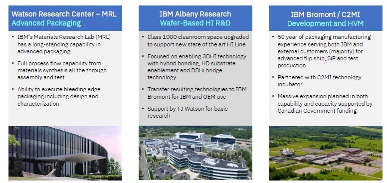
IBM announced that upcoming expansions were to be expected. Phase 1 (production ramp 2024) would increase assembly and test capacity for FcBGAs. Phase 2, in collaboration with C2MI — which is owned by the Canadian government but run by IBM — will bring up “…an R&D and manufacturing facility that will offer capabilities and manufacturing capacity to match and exceed existing Asian capabilities in advanced packaging.” Phase 2 will offer a complete North American supply chain solution for high-end advanced packaging.
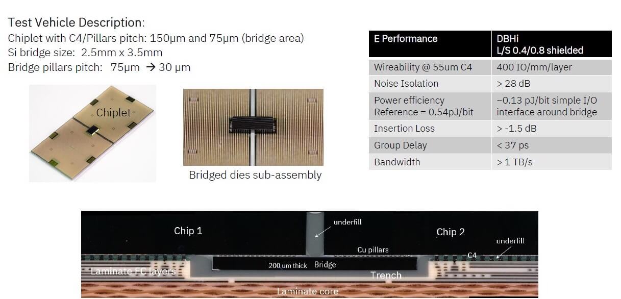
One of the IBM technologies that they will be scaling up will be its heterogeneous integration (DBHI) which is shown in Figure 2. This is IBM’s silicon bridge technology, which appears easier to manufacture than Intel’s EMIB technology. Janta-Polczynki indicated that this technology will be available to all customers through IBM Bromont.
In terms of chiplet module assembly, Janta-Polczynki commented that IBM is ready in the areas of module design, module assembly, and test, as well as characterization and modeling.
Ajinomoto Fine-Techno Next-Gen ABF
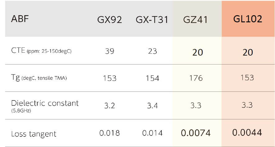
Ryohei Oishi of Ajinomoto Fine-Techno discussed “Advanced Insulation Materials Designed for High-Density Package High-Speed Applications,” focusing on low-loss Ajinomoto Buildup Film (ABF) for high-frequency packages and next-generation ABF for thinner HI packaging and fan-out wafer level packaging (FOWLP).
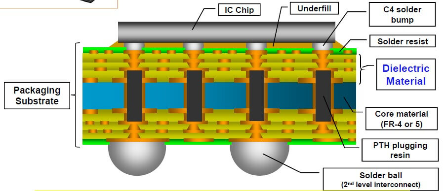
As a review, ABF has become the de-facto standard dielectric material for CPU/MPU packaging substrates (Figure 3).
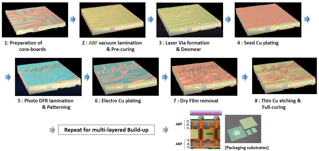
The ABF process flow is shown in Figure 4.
- The GX series consists of epoxy and a phenol hardener.
- The GZ series consists of epoxy and cyanate ester.
- The GL series consists of epoxy and phenolic ester hardener.
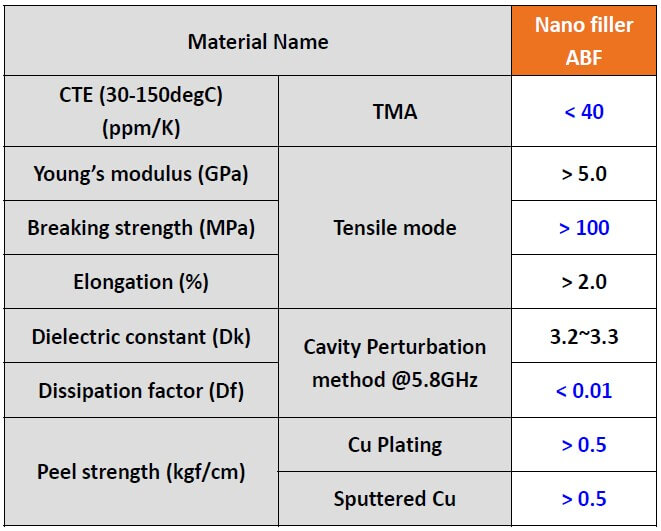
The next-generation materials for thinner applications use GL chemistry with nanofillers (Figure 6).
Subu Iyer to head CHIPS NAPMP

Professor Subramanian Iyer has been named Director of the National Advanced Packaging Manufacturing Program (NAPMP) at the US Department of Commerce (NIST). He will be on an IPA assignment from UCLA for an initial period of two years. Before accepting his position at UCLA, Subu spent the bulk of his career at IBM.
The CHIPS for America R&D Office is responsible for four integrated programs that will ensure American semiconductor manufacturers remain globally competitive: the National Semiconductor Technology Center (NSTC), the NAPMP, up to three new Manufacturing USA institutes dedicated to semiconductors, and the CHIPS R&D Metrology Program.

The NAPMP aims to accelerate the development and implementation of assembly, packaging, and test capabilities in the domestic microelectronics ecosystem by identifying leap-ahead technologies that will place U.S. advanced packaging in a globally competitive position.
IFTLE supports this surprisingly excellent choice!
Dev Palmer was Promoted within DARPA

Dr. Dev Palmer was recently promoted to Managing Director of next-generation Microelectronics Manufacturing at the Defense Advanced Research Projects Agency (DARPA).
Palmer was named Deputy Director of the Microsystems Technology Office (MTO) in April 2020. Prior to that, he was Chief Technologist at the Lockheed Martin Advanced Technology Laboratories.
He served tours as a program manager in MTO from 2012 to 2017 and at the US Army Research Office Electronics Division from 2001 to 2012. In both positions, he directed a portfolio of research and development programs driving innovation for next-generation systems for radio communications, sensing, and electronic warfare. His career in defense-related research and development began at the Microelectronics Center of North Carolina (MCNC), where he worked from 1991 to 2001, ultimately serving as director of the Optical and Electronic Packaging Group.
For all the latest in Advanced Packaging stay linked to IFTLE……………………….


