This week, we continue our look at the presentations at the IMAPS CHIPCon conference that was held at the end of July 2023. Here we focused on process tools and EDA for chiplets.
Hybrid Bonding at Besi
Besi is a global leader in equipment for advanced packaging assembly and equipment for leadframe, substrate, and wafer-level packaging applications in a wide range of end-user markets including electronics, mobile internet, cloud server, computing, automotive, industrial, LED, and solar energy. According to the Besi website, the company has ~1800 employees with over 70% of them in Asia. 2022 revenue totaled 722M Euro.
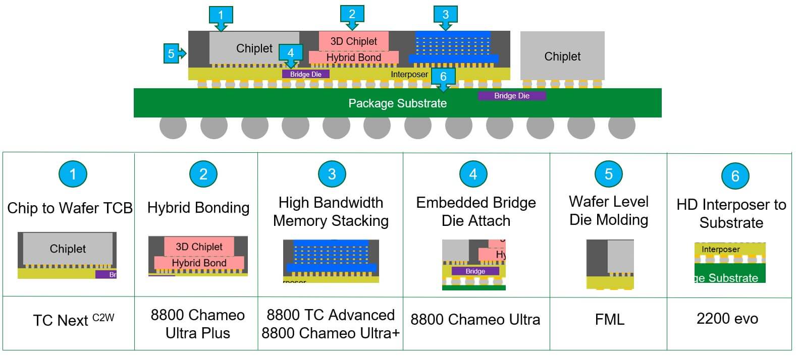
In his keynote presentation Tom Strothman, Besi discussed “Die to Wafer Hybrid Bonding for Heterogeneous Integration”. He pointed to the fact that new chiplet 3D structures use a variety of advanced packaging assembly processes as shown in Figure 1.
Tom noted that hybrid bonding was on the manufacturing roadmap for all the major players such as TSMC, Samsung, AMD, Intel etc. Hybrid bonding is a game changer for increasing contact density as shown in Figure 2.
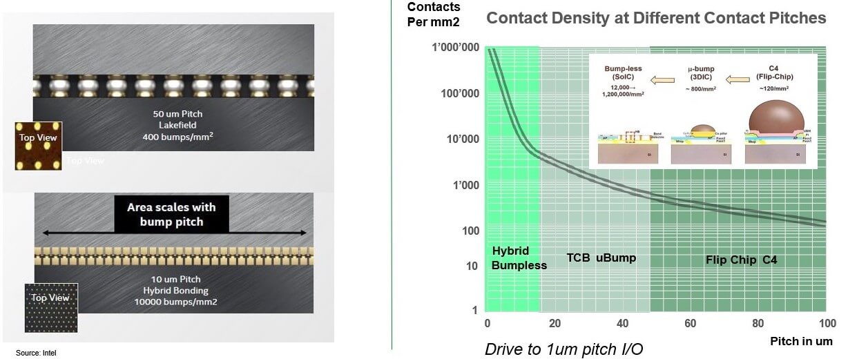
Strothman quoted Yole’s prediction that hybrid (HB) will be used for HBM die stacking beginning with HBM4, and that 36% of HBM will use hybrid bonding by 2028.
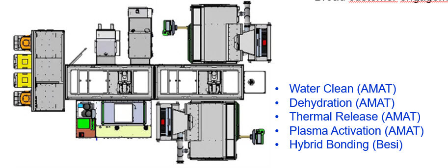
He said that Besi’s die-to-wafer (D2W) HB tool is currently showing +/- 0.3um placement accuracy. The company currently has a joint development with AMAT for a complete HB assembly system as shown in Figure 3.
Kulicke & Soffa (K&S) Processes
Peter Van Emmerik discussed K&S’s new fluxless thermocompression bonding (TCB) processes.
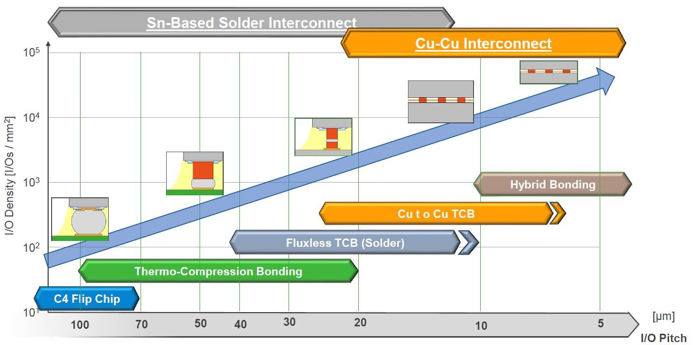
A valuable slide is an update of the interconnect slide that most of us have been using for the past few years. This now shows, in their opinion, the points of introduction for TCB and HB.
The company developed fluxless TCB because “thorough cleaning of large chip areas with small chip gaps and/or high density interconnects can be challenging and time-consuming” (Figure 5). Their process basically uses a formic acid oxide reduction of SnO similar to what has been done in the past for copper oxide reduction.
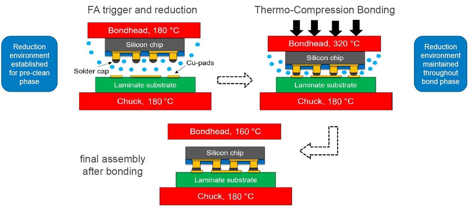
Figure 5: Example of In-situ formic acid TCB Process Flow (Source: K&S)
Siemens EDA for Chiplets
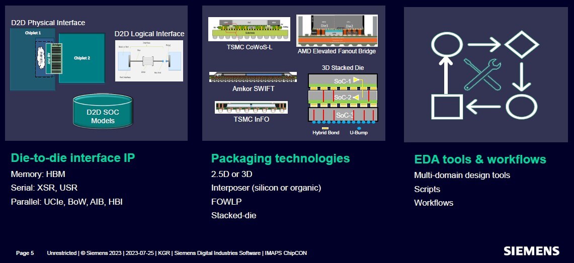
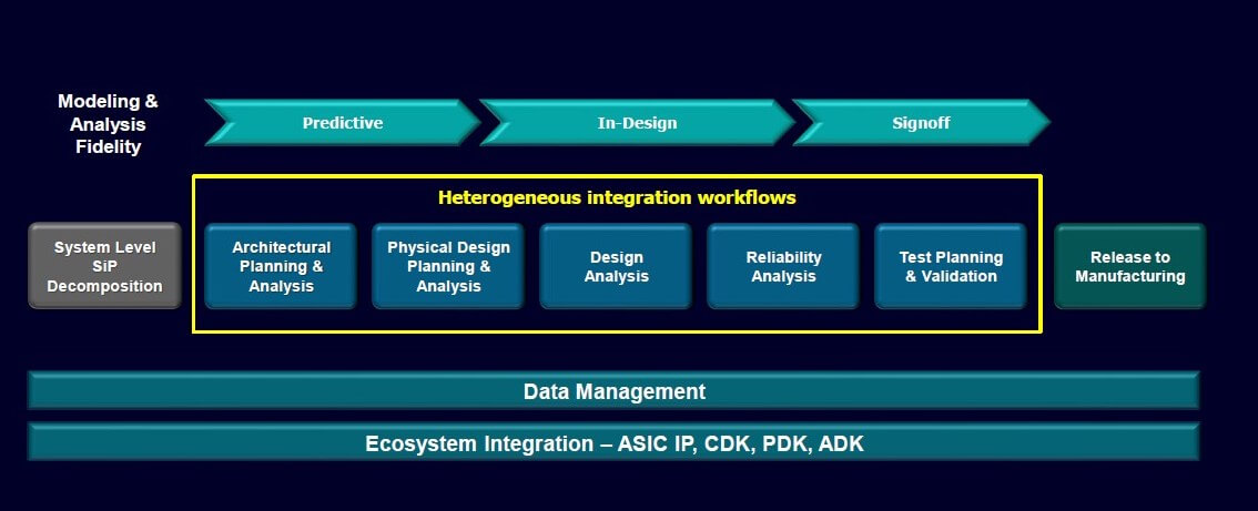
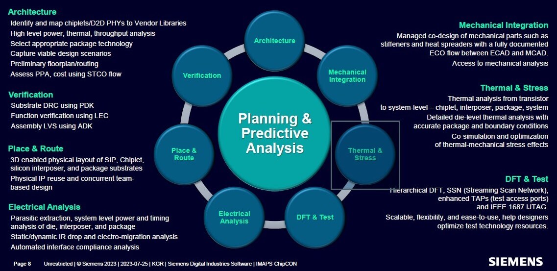
Kevin Reinbold of Siemens EDA discussed “Workflows for tackling Heterogeneous Integration (HI) of chiplets for 2.5/3D”.
Cadence
John Park of Cadence discussed “Chiplet/Package Co-design / Analysis Challenges and Opportunities”. He said that technological breakthroughs in advanced packaging have been the key to enabling chiplet-based systems in package architectures. IC and system designers have been forced to work together to develop “co-design” methodologies. Co-design is explained below in Figure 9.
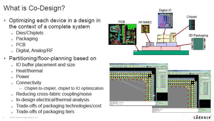
Park then goes through a discussion of the modern methodologies that are now enabling co-design as is schematically shown in Figure 10:
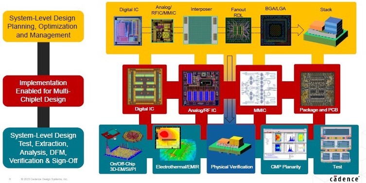
Figure 10: Modern methodology enabling co-design.
For all the latest in Advanced Packaging stay linked to IFTLE………………………