

Also: US CHIPS Seeking < $300M Proposals
TSMC’s Offshore Fabs
Nikkei Asia is reporting that TSMC’s $8B Japan chip project steams ahead as its U.S. site continues to hit snags. TSMC has launched significant global expansion in the U.S., Japan, and Germany to address growing customer demand and diversify production footprints. TSMC Chairman Liu says the company needed to globalize to retain and expand its technology and manufacturing leadership.
The capacity of TSMC’s offshore fabs being built overseas accounts for less than 10% of its total capital investment. TSMC’s latest Global Production capacity as described by Trendforce is shown in Figure 1.
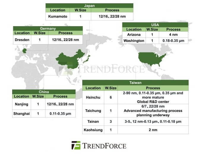
TSMC’s offshore fabs include the Arizona fab, the fab it is building in Kumamoto, Japan, and the fab it is going to build in Germany. They are all different in location, setup, and scope.
Tool installation at TSMC’s Japan Kumamoto plant started in October 2023 with production to begin in 2024. TSMC has begun installing equipment at its new chip plant in Japan indicating that the project is proceeding more rapidly than the company’s cutting-edge facility in the U.S. The $8 billion plant is on track to meet its target of beginning production by the end of next year and may even be ahead of schedule. The Kumamoto project was announced in October 2021, construction began in 2022 and mass production is expected in 2024. The Kumamoto plant will start out using 28-nm and 22-nm production technology, which is relatively mature and can churn out chips such as image sensors, driver-integrated circuits, and microcontrollers that are used in everything from smartphones to cars.
TSMC has reportedly sent hundreds of support staff to the site in Japan, to be joined by hundreds more from TSMC suppliers. TSMC has told several suppliers that the installation of chip production tools will be completed in the first quarter of 2024.
The chipmaker has also sent several hundred “seed” employees experienced in running such plants to Japan since the summer, as well as hiring locally to prepare for plant setup. Suppliers dispatched another few hundred engineers to help set up the facility in October. The Japanese government has reportedly streamlined regulations that enable TSMC to bring up its supply chain and work faster. TSMC indicated that “the Japanese industry has a very strong ecosystem in materials, gas, substrates, and wafers. Having access to that is very strategic.”
The relatively smooth progress at TSMC’s first chipmaking facility in Japan stands in stark contrast to its plant in Arizona, in the US, which will eventually produce 4-nm chips. Plans for the Arizona facility started in mid-2020, construction began the following year, and production, which was originally slated to begin in 2024, has been pushed back to 2025.
“In each site, we work closely with our customers, partners, and vendors to understand cost, labor, and regulatory factors and move forward accordingly.”
Reports indicate that Japan has better chip industry infrastructure than the U.S. and has been more prompt with government support. Japan has already earmarked $3.5B worth of subsidies for the TSMC project. The U.S. only finalized the CHIPS Act, a package of support for the industry, in the last few months and has yet to allocate its funds. In addition, the US CHIPS Act restrains recipients from expanding chip manufacturing in “countries of concern” for 10 years.
U.S. regulations are more complicated, he said, making it difficult for TSMC to bring its more than 100 suppliers to work with it in Arizona. The slower allocation of American subsidies could also increase the time it takes chipmakers to install equipment in new plants.
Others have noted the working culture in Japan and Taiwan as a factor behind the Kumamoto project’s progress, along with fewer logistics hurdles. Reports indicate that “Culturally, Japanese and Taiwanese workers are more accepting of long, grueling work hours and monthly schedules that most American workers will find hard to live with.”
Chairman Mark Liu acknowledged that TSMC has had to experience a “learning curve” during this overseas expansion.

A key Japanese equipment supplier who is familiar with TSMC’s expansion in Taiwan, Japan, and the U.S. states that “… In Taiwan, it’s possible to hoist semiconductor equipment in just one day with a crane, while in Japan, it might take two or three days. In the U.S., it might take more than a week. This affects the speed of building the factory.”
There is also the problem of finding enough qualified workers in all three locations, according to Capri of the Hinrich Foundation. “Engineers, physicists, computer scientists, and other skilled positions are in short supply for the chip sector.”
CHIPS for America Small-Scale Supplier Project Funding
 CHIPS for America has announced that it is accepting small-scale supplier project concept plan submissions in the application portal (2023-NIST-CHIPS-SMME-01).
This funding opportunity seeks applications for projects for the construction, expansion, or modernization of commercial facilities for semiconductor materials and manufacturing equipment with capital investments of less than $300 million.
The application process includes two primary phases. In the first phase, applicants will be asked to submit a concept plan describing how their proposed project addresses core program priorities. Concept plans will be accepted between December 1, 2023, and February 1, 2024. The Department will then invite the most promising applicants to the second phase.
The Department is particularly interested in applications that advance clusters by closing critical gaps in the U.S. supplier landscape. If a project does not support a cluster, the application must make a compelling case for advancing one of the Department’s other two objectives. will have the opportunity to submit a full application.
The Concept Plan should be at most 2 pages. Applicants should provide a detailed description of the project and the applicant. Please note, most of this information will also be collected in the web portal. The list below outlines the basic requirements:
Project Description
- Describe the construction, expansion, or modernization activities proposed.
- Describe what will be produced and their end market applications.
- Describe the scale, size, and capacity of production.
- Applicant Description
- Applicant profile
For all the latest in Advanced Packaging activity satay linked to IFTLE……………


