A recent Wall Street Journal article, The Microchip Era Is Giving Way to the Megachip Age, explains how the chip industry is transitioning from monolithically integrated chips to stacking chiplets to make megachips. In the U.S., DARPA is embarking on the Next Generation Microelectronic Manufacturing initiative focused on three-dimensional heterogeneous integration (3DHI) microsystems, and the CHIPS and Science Act of 2022 aims to strengthen American semiconductor manufacturing, supply chains, national security, and R&D. There are also similar government initiatives in Europe and Asia.
The fly in the ointment is a shortage of skilled workers to develop and manufacture these megachips, so workforce development is a critical need. Below are some important considerations for workforce development that I’ve learned from my career:
- Future: Forty years ago, when I was a freshly minted mechanical engineer working for General Electric, I had no idea what to do with my career. When I had the opportunity to work on a microprocessor-based gas turbine control system, the lightbulb went off and I realized that working in the semiconductor industry is a great career.
- Fun: Early in my semiconductor career, I was fortunate to work closely with many charismatic, entrepreneurial executives. COMDEX, the annual computer expo trade show in Las Vegas, drove a huge sense of urgency. Many great friendships were formed as people came together to brainstorm ideas, take risks, and do whatever needed to get done to make their COMDEX deadline.
- Community: I could take on risky, cutting-edge projects because I had job security, but not from my employer. It was because I was part of a larger local community, and I worked with people at many related companies. So, if my project or my employer failed, I could start working the next day for another nearby company.
- Pivot: Every successful lab-to-fab transition I was involved with went through one (or more) pivots. Plan-the-work-and-work-the-plan never worked! Our first plan generally failed, so we had to quickly make some mid-course corrections.
- KISS (Keep It Simple, Stupid): Also, every successful lab-to-fab transition I saw first commercialized a “minimum viable product” – a simple baby step in a new disruptive product family.
We need to provide our next generation of potential engineers with clarity that the semiconductor industry provides many attractive career opportunities. Such clarity best comes from first-hand, hands-on experience. Ideally, such experience includes working with a small, entrepreneurial team on a minimal viable product, executing mid-course corrections, developing friendships, having fun, becoming part of a community, and contributing to society,
Where Megachips Factor In
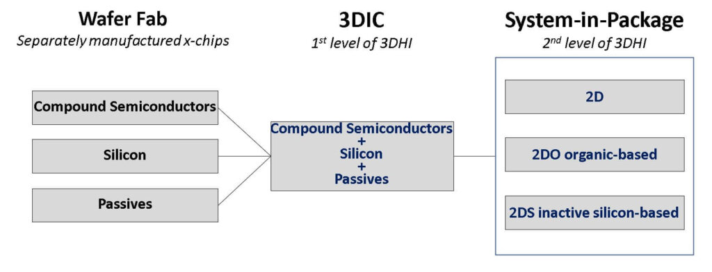
Megachips do indeed offer many opportunities because they have a wide range of technical and economic barriers that require innovative solutions. Some megachips will integrate a trillion transistors in a system-in-package (SiP) by the end of the decade. Today’s megachips use heterogeneous integration of different silicon nodes to address the yield and memory barriers by disaggregating large silicon die into arrays of smaller (hence, higher yield) chiplets and stacking logic and memory chiplets, respectively.
The remaining technical barriers that constrain megachip performance include communications (getting data in and out of megachips), power delivery (improving energy efficiency by supplying many precise voltage rails), and thermal management (removing heat). Solutions to these technical barriers require heterogeneous integration of non-silicon materials (e.g., compound semiconductors, thin-film passives, and heat spreaders) for ultra-thin optical and RF communications, power management, and thermal management components. A major economic challenge is that hundreds of millions of dollars are required to develop a new product using advanced CMOS monolithic integration. Only a small number of products are developed by just a few very large companies because each product development is a “too big to fail” effort that must generate huge revenues with low risk.
To democratize megachips so that we avoid these issues, the winning strategy is to disaggregate megachips into many separately manufactured components that may be assembled together in a mix-and-match fashion, like Lego blocks. Promising approaches include using multiple levels of 3DHI (Figure 1). The first level produces a “minimum viable product” 3DIC that is a thin, tested known good “die.” This approach integrates multiple materials and process technologies versus building a monolithic die and bridges the interconnect gap between the fine, but thin wafer fab interconnects and the much coarser, thicker SiP interconnects. The second level uses advanced packaging technology to integrate many thin 3DICs into the SiP.
Micro-transfer Printing Method
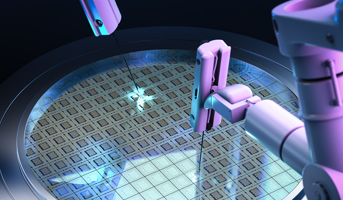
A proven method for manufacturing 3DICs that heterogeneously integrate compound semiconductors and silicon is micro-transfer printing technology (MTP). MTP heterogeneously integrates compound semiconductors and silicon in a massively parallel pick-and-place process that efficiently transfers large arrays of ultra-thin (<20mm), small, separately manufactured components (x-chips), from one or more source wafers to destination substrates. The MTP manufacturing steps are:

- Fabricate the destination substrate, which may be a silicon wafer with integrated CMOS ICs, silicon, glass, or ceramic interposer wafer, or a large-area glass panel.
- Fabricate the source wafers with tightly packed x-chips made using the optimal process node and technology (such as SOI, GaN, GaAs, InP, or SiGe) with a sacrificial layer formed underneath and a tether/anchor system to suspend the x-chips after the source wafer is anisotropically etched to remove the sacrificial layer.
- Etch the release layer using standard MEMS technology.
- Fabricate the MTP elastomer stamp using a low-cost, reusable mold. The MTP stamp contains an array of soft posts composed of a compliant elastomer material, polydimethylsiloxane (PDMS), on a stiff glass substrate. The stamp is stiff in the x-y dimensions, providing high placement accuracy, and compliant in the z-dimension, accommodating non-planar and rough destination substrates
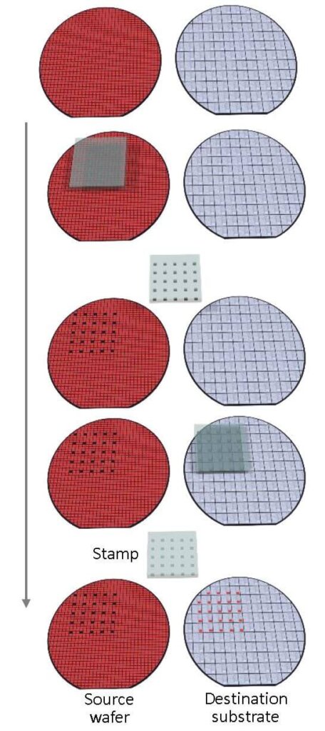
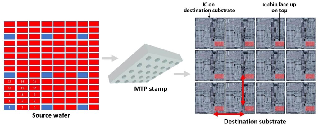
- Use the MTP system for massively parallel pick-and-place of x-chips active-side up from the source to the destination substrate (Figure 2). The post array on the stamp (Figure 3) is customized to match the desired destination substrate locations for massively parallel, selective pick-and-place of thousands of x-chips. The stamp’s posts adhere to the x-chips via van der Waals force. The stamp’s viscoelastic behavior uses fast separation speed during pick-up to break the tethers and remove the x-chips, and slow separation speed to place the x-chips on the destination substrate. Using a “step and repeat” process, the entire destination substrate is populated with x-chips.
- Figure 3: MTP Stamp’s Post Array Customized for Selective Pick-and-Place
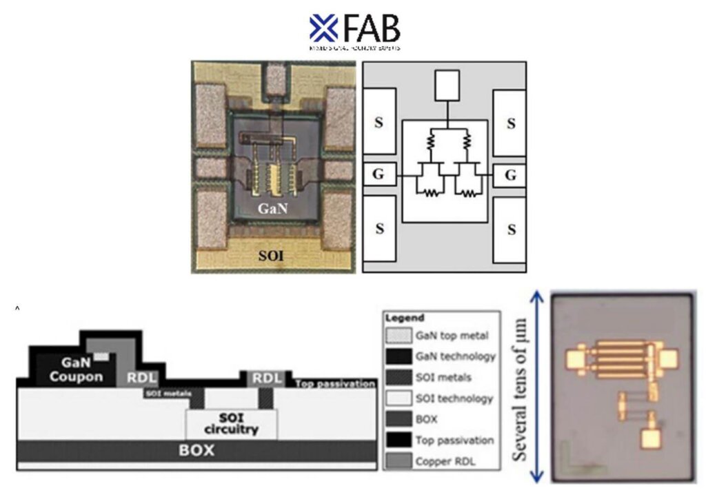
Since the x-chips are ultra-thin and active side up, standard copper redistribution layer (RDL) technology may be readily used to interconnect the x-chips and destination die (Figure 4), resulting in very short path lengths and, hence, minimum parasitics. A multi-level RDL provides a low electrical and thermal resistance path and enables use of multiple advanced packaging options for the second level. MTP is well-suited for photonics, GaN and silicon heterogeneous integration for RF and power management, and other compound semiconductor 3DICs.
How MTP Facilitates Workforce Development
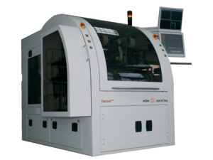
It is straightforward and cost-efficient for universities, research organizations, startups, and large companies to add MTP to their existing facilities since both ASM AMICRA and X Display Company supply R&D and production MTP manufacturing systems (Figure 5). MTP systems are installed at X-FAB, Micross Components, Tyndall National Institute / PIXAPP, Teledyne, the Naval Research Laboratory, the University of Illinois Urbana Champaign, the University of Ghent / imec, UPVfab (the microfabrication facility at the Universitat Politècnica de València), and several undisclosed leading manufacturers. More than twenty MTP systems are installed worldwide.
MTP is an example of a readily accessible, cutting-edge technology that can facilitate workforce development. The technology enables students to gain hands-on experience through mixing and matching separately manufactured components produced in various external wafer fabs to produce compound semiconductor 3DICs that tackle megachip’s communications, power delivery, and thermal management challenges.