
In the rapidly evolving microelectronics landscape, demands for higher performance, reduced size, and faster development cycles are driving the industry toward more innovative design paradigms. This was traditionally accomplished by miniaturizing transistors within microprocessors as was described by Moore’s Law. Gordon Moore of Intel estimated that the number of transistors in an integrated circuit will double every two years, which has been true for the last 60 years, but physical limits are beginning to be met and alternative methods to driving innovation are needed. Chiplets are the newest method to continue driving progress forward in the spirit of Gordon Moore. One such innovation is the chiplet architecture—a modular approach that disaggregates traditional system-on-chip (SoC) designs into smaller, independently manufactured, reusable chip sets. This approach is transforming how integrated systems are built, offering significant advantages in flexibility, scalability, and system performance.
During the Micross webinar held on May 1, 2025, industry experts came together to provide deep insight into the advantages and design considerations of chiplets, especially in high-reliability systems. The session explored the current state of the chiplet ecosystem, challenges surrounding standardization, and how chiplets are enhancing device integration, SWaP (Size, Weight, and Power) performance, and time-to-market.
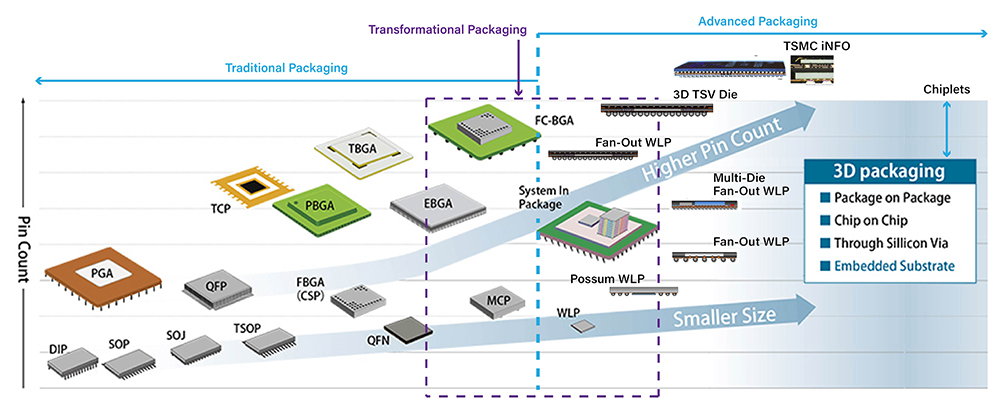
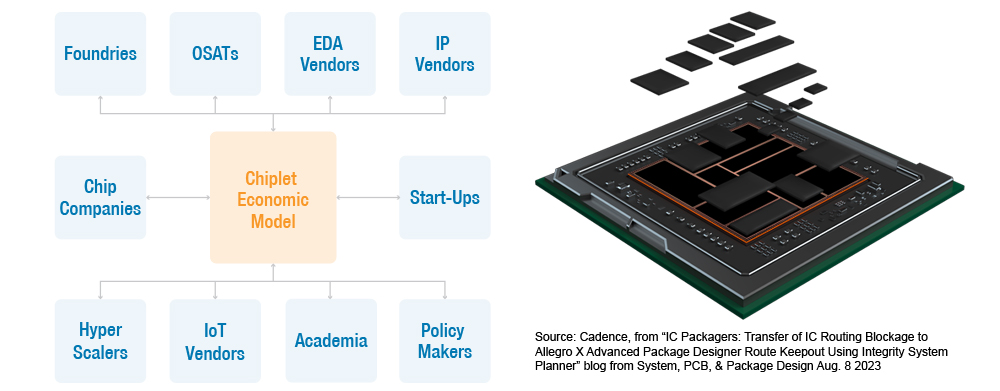
The Chiplet Paradigm: Addressing Modern Market Needs
Chiplets offer a compelling alternative to monolithic semiconductors by partitioning complex systems into modular die components, each optimized for specific functions (e.g., compute, I/O, memory, RF, analog). These can be independently fabricated using different materials and process technologies that are later assembled into a unified system using 2.5D and 3D integration.
Optimized Device Integration Through Heterogeneous Architecture
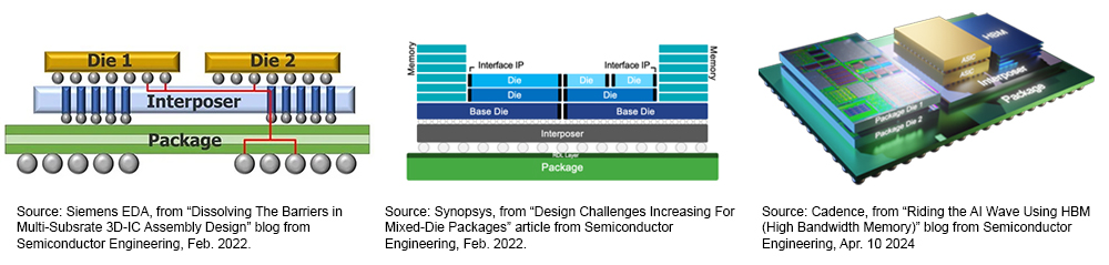
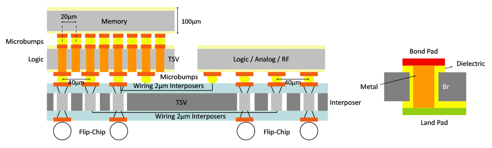
Chiplet-based architectures support heterogeneous integration, wherein components with varying materials, linewidth nodes, and functionalities are co-packaged. This method enables system designers to optimize performance by using the best technology for each system. 3D heterogenous integration requires wafer bumping, redistribution layers (RDLs), Through silicon vias (TSVs), silicon or glass interposers for direct connectivity, reducing latency and power losses and eliminating wire bonds.
Enhancing SWaP Performance with Modular Design
By decoupling the development of individual chiplets, designers can iterate on subsystem improvements independently, further driving performance gains without redesigning every node within a traditional system on a chip.

Accelerating Time-to-Market and Reducing Development Costs
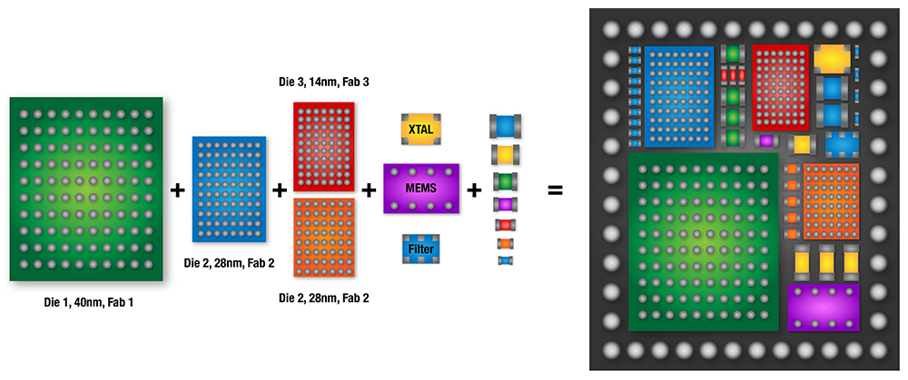
Chiplets leverage the best of multiple companies’ technology and integrate them into a single component. This can be as simple as stacking memory die next to processors or can become as complicated as an entire RF system with transmit and receive signal chains.
Current Challenges: Standardization, Testing, and Interoperability
Chiplets standards are evolving for interconnects, communication protocols, and packages. Currently, no universal industry standard defines how chiplets from different suppliers should interconnect or communicate. This fragmentation hinders interoperability and makes vendor lock-in more likely. While efforts like UCIe (Universal Chiplet Interconnect Express) are underway to unify the space, broad adoption is still evolving.
Unlike monolithic chips, chiplets require both individual die testing and system-level validation after integration. This demands specialized test infrastructure and methodologies. Known-good-die (KGD) is the dominant approach, where each chiplet is fully tested before assembly to avoid yield losses at the package level.
Best Practices for Chiplet Designs
- Start with Reuse in Mind: Design chiplets to be modular, scalable, and compatible with future system iterations.
- Invest in Testing Infrastructure: Ensure access to advanced die-level and system-level test solutions to maintain yield and reliability.
- Design for Interoperability: Where possible, follow emerging standards (e.g., UCIe) to future-proof systems against ecosystem fragmentation.
- Collaborate Across Domains: Encourage cross-functional collaboration among foundries, designers, packaging, test, and reliability teams from the outset.
- Leverage Trusted Suppliers: Partner with experienced and secure supply chain providers who have deep domain experience in 3D integration of chiplets.
Chiplets are playing an essential role in microelectronics innovation, fueling the next 60 years of Moore’s Law. Gain deep insight into the considerations and best practices in leveraging the value and performance of Chiplets for high-reliability systems, view the recorded Chiplets Webinar now.


