
From the cloud to edge computing, the quest for ever-greater power efficiency remains researchers’ top priority. From high-end niche to mass-market applications, the best cost-to-performance tradeoff is key to providing a competitive advantage. While Moore’s Law has helped meet the performance required in terms of data transfer and power efficiency so far, including for high-end applications such as high-performance computing (HPC), it is no longer relevant when it comes to cost-sensitive applications such as edge artificial intelligence and internet of things (IoT) devices.
This presents researchers with difficult choices: can they afford to pursue advanced node performance? Must they find a trade-off, with a risk of inhibiting product performance? And can heterogeneous integration be the solution that will enable decades of future innovation?
CEA-Leti researchers may not have a final answer yet, but their recent results in this technique, including die stacking and monolithic 3D integration, suggest a potential way through the cost/performance dilemma.
Heterogeneous strategies: From greater density…
Vertical 3D integration technology enables stacking chips in a device to help achieve denser interconnects, which translates into greater power optimization and an improved signal propagation within the component. The die-to-wafer (D2W) direct hybrid-bonding process using copper/oxide mix interfaces has been identified by major microelectronic industrial companies as essential for the success of future logic and memory stacks, thanks to its promising low interconnection pitch and known good die (KGD) selection capabilities.
Last year, CEA-Leti demonstrated D2W hybrid bonding with 10µm interconnection pitch and a simple process adapted from its wafer-to-wafer (W2W) expertise. The latest major advances in die-bonding-alignment capability through its collaboration with SET paves the way to reach 5µm interconnection pitch. Exploratory work on the process of reducing the alignment to <1µm has already been demonstrated in the development of a self-assembly process. In November 2020, the institute demonstrated proof-of-concept of the KGD approach, compatible with direct hybrid bonding, that involves selecting high-topography tested chips (>2µm) and transferring them to direct bonding that tolerates a maximum topography of 10nm. This was made possible thanks to researchers’ deep expertise in planarization.
…to greater flexibility
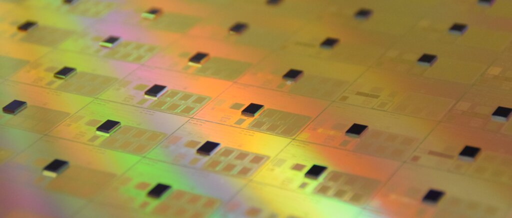
Beyond power and interconnections, 3D technology also allows for the manufacture of more efficient, thinner, and lighter microprocessors. In addition, by implementing multiple heterogeneous solutions in a single package, chip companies benefit from considerable flexibility, allowing them to mix and match technology blocks with IP and integrate memory and input/output (IO) technologies within the same component. A good example of this is the collaboration between CEA-Leti and Intel. Their research focuses on the assembly of smaller chips, the optimization of interconnection technologies between the different elements of microprocessors, and on new bonding technologies and stacking for 3D integrated circuits (3D ICs), in particular for the realization of HPC applications, by leveraging advanced 3D packaging technologies (Figure 1).
Enabling high-performance processors to power exascale computing
Computing performance has grown exponentially in recent decades. This has led to HPC opening the door to new horizons and allowing for the resolution of extremely complex problems that require processing vast amounts of data. Supercomputers will soon achieve exascale-level computing performance: 1018 flops, or one-billion-billion floating-point operations per second.
However, in the context of HPC, the integration of greater computing capacities with generic cores or dedicated accelerators for AI applications comes with significant challenges. Manufacturing yield and costs remain the main hurdle. 3D technology appears as a clear alternative to More than Moore, offering a matrix, and modular and robust architecture.
3D integration and quantum computing
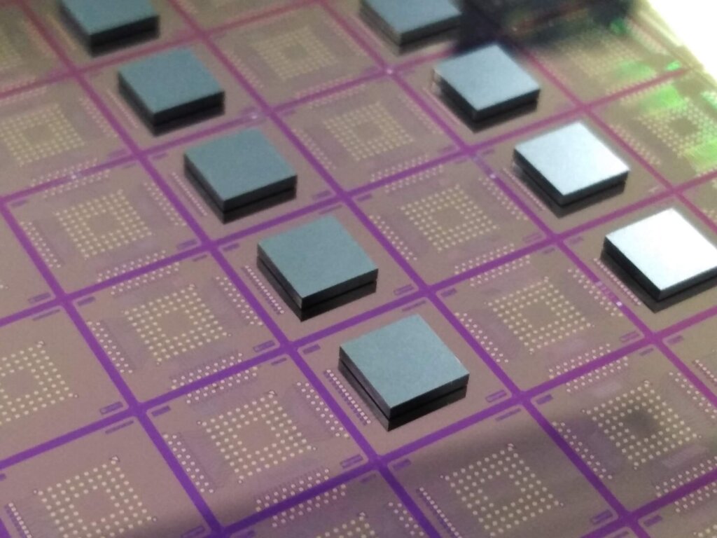
In 2019, CEA-Leti developed INTACT, a proof-of-concept integrating 96-core architecture comprising six chiplets (FDSOI 28nm node) 3D-stacked on an active silicon interposer (CMOS 65nm node) (Figure 2). Following this achievement in the HPC domain, similar architectures are envisioned for quantum computation to vastly improve performance and speed. A team of scientists from CEA-Leti, CEA-List, and the Néel Institute at the National Center for Scientific Research (CNRS) designed the first prototype interposer in 2020.
The interposers’ primary purpose is to accommodate and connect quantum chips containing qubits and control chips used to address and read the qubits (two-level storage units for quantum computing using the same approach as for HPC requirements). Known as QuIC3, which stands for quantum integrated circuits with CryoCMOS, this prototype demonstrator is an important step towards the realization of a complete quantum computing system.
CoolCube™: About CEA-Leti’s monolithic 3D technology
Since 2016, CEA-Leti has extended its 3D integration roadmap with its CoolCube® technology in which stacked FDSOI transistors are interconnected with pattern alignment accurate to the nanometer, which is what makes all the difference compared to 2D technology. This also allows an increase in the density of the components without reducing their dimensions. As an extension of high-density 3D Cu-Cu/hybrid bonding chip-to-wafer/wafer-to-wafer technologies, CoolCube™ enables stacking active layers of transistors in the third dimension, while coping with thermal budgets that do not degrade the performance of transistors or metal interconnects. CEA-Leti works on various 3D very-large-scale integration (VLSI) advanced concepts, which have broad applications in low-power mobile devices and other IC platforms.

In June 2020, in an FDSOI CMOS processing breakthrough, CEA-Leti pushed fabrication thermal-process boundaries down to 500°C for CMOS integration, while showing strong performance gains, especially in p-type metal-oxide-semiconductor (PMOS) logic devices. The 500°C threshold is important because in 3D monolithic technologies (also called 3D sequential), fabricating the upper-level transistors at higher temperatures than that can damage the metal interconnects and the silicide of the bottom-level transistors. Using CEA-Leti’s CoolCube® low-temperature process for top-level devices prevents deterioration of bottom-level transistors.
CEA-Leti has recently exploited the CoolCube® technology to increase the density of resistive memory arrays by fabricating monolithically integrated multiple one-transistor/one-resistor (1T1R) structures, reducing the cell size by 1.5x with respect to planar 1T1R. The proposed 3D monolithically integrated multiple 1T1R cells have been combined with multilevel cell programming to further enhance memory density.
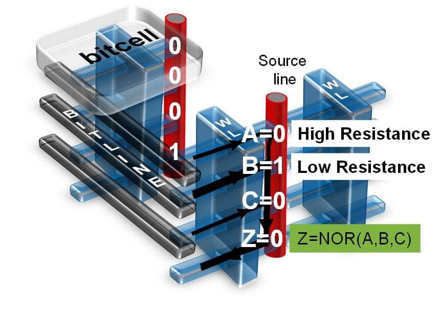
Improving 3D technology also means imagining and designing new 3D architectures. Developed by S. Barraud et al. at CEA-Leti in collaboration with the University of Aix-Marseille, a new 3D memory cube architecture composed of nanosheet gate-all-around (GAA) transistors stacked vertically makes it possible to overcome the limitation in the size of cells imposed by a conventional transistor. This new type of stacking, developed for advanced CMOS, has excellent 3D integration scalability (Figure 3).
CEA-Leti and its partners have demonstrated along with the year’s relevance of 3D architecture for high-performance applications by leveraging a wide range of technologies, from direct hybrid bonding, sequential 3D integration, to silicon interposer. The future is vertical.
Editor’s Note: This article first appeared in the 2021 Yearbook. Read the issue here.
Learn more:
- Die to Wafer Direct Hybrid Bonding Demonstration with High Alignment Accuracy and Electrical Yields, Jouve A. et al., 3DIC 2019
- Towards a Complete Direct Hybrid Bonding D2W Integration Flow: Known-Good-Dies and Die Planarization Modules Development, E. Bourjot et al., 3DIC 2019
- Self-Assembly Process for 3D Die-to-Wafer using Direct Bonding: A Step Forward Toward Process Automatisation, Jouve A. et al, 2019 IEEE 69th Electronic Components and Technology Conference (ECTC), Las Vegas, NV, USA, 2019, pp. 225-234, doi: 10.1109/ECTC.2019.00041.
- Known Good Dies (KGD) strategies compatible with Die-To-Wafer Direct Hybrid bonding CEA-Leti: Bourjot, P. Stewart, N. Bresson, L. Sanchez, C. Castan, G. Mauguen, Y. Exbrayat, V. Balan, F. Fournel, S.Cheramy, P. Vivet SET Corporation: N.Raynaud, P.Metzger
- CEA-Leti Announces Collaboration with Intel to Advance Chip Design Through Cutting-Edge 3D Packaging Technologies. https://www.leti-cea.com/cea-tech/leti/english/Pages/What-s-On/CEA-Leti-Announces-Collaboration-with-Intel-to-Advance-Chip-Design-Through-Cutting-Edge-3D-Packaging-Technologies.aspx
Part of this work was been developed in the frame of IRT Nanoelec. - How 3D Integration Technologies Enable Advanced Compute Node for Exascale-Level High-Performance Computing? Dutoit et al. IEDM 2020
- Die-to-Wafer 3D Interconnections Operating at Sub-Kelvin Temperatures for Quantum Computation; C. Thomas and al. ESTC 2020.
- French Team on Route Towards an Interposer Prototype for Quantum and Control Chips Integration at Very Low Temperature (CEA-Leti Press Release, Nov. 2020)
- CEA-Leti Scientists Demonstrate CMOS Device Fabrication at 500°C, Paving the Way to High-Performance 3D Monolithic CMOS Integration
- 3D RRAMs with Gate-All-Around Stacked Nanosheet Transistors for In-Memory-Computing, Barraud et al, IEDM 2020
- High-Density Multi-Level-Cell 3D Sequentially Integrated 1T1R RRAM Array for Neural Networks, Esmanhotto et al, IEDM 2020
- 3D Sequential Integration: Opportunities, Breakthroughs, and Challenges IEDM 2020 Short Course Session 1 by Claire Beranger-Fenouillet
- This work was partly supported by the European Union’s Horizon 2020 research and innovation program under Grant Agreement No. 820048 (ERC My Cube); No. 295970 (ANDANTE), No. 826655(TEMPO), and No. 871371 (MeMScales).
Note: Part of this work was developed in the frame of IRT Nanoe