

IFTLE (Insights From the Leading Edge), believe it or not, has reached #500! I hope this message reaches all of you free of COVID and ready to move on in this exciting period for Advanced Microelectronic Packaging. For those of you that have not been on board for the full trip, let me share a little background history.
Background 2004-2010
After retiring early in 2004 following a 27-year career at Dow Chemical, I started writing Advanced Packaging articles for Pete Singer and his leading microelectronics magazine of the day “Semiconductor International” (SI). While SI’s main focus was on front-end chip fabrication, there was readership interest in the leading packaging technologies of the day.
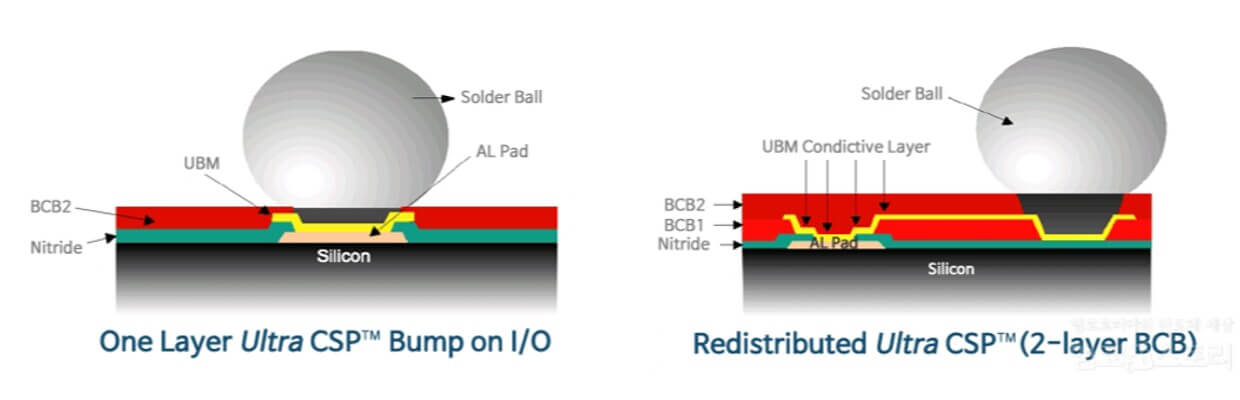
Post-2000 wafer-level packaging (WLP) was just beginning to catch on as Pete Elenius and Flip Chip Technology (FCT) began licensing its bumping and WLP technology to all the major packaging houses in Taiwan and Korea. WLP was of special interest to me since, while at Dow, my electronics business had helped FCT develop its “Ultra CSP” WLP and low-cost bumping technologies with our Benzocyclobutene resin (BCB).
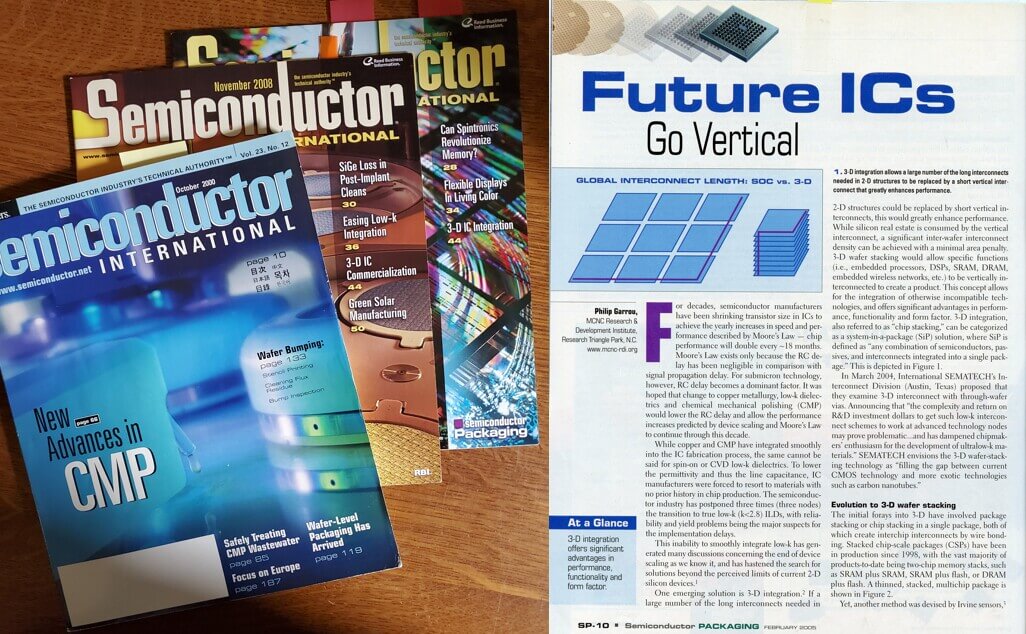
In 2005 Kenny Williams at the Microelectronics Center of NC, hired me part-time to help with its new DARPA 3DIC program and I quickly became convinced that vertical integration was the next big thing. I knew from the beginning that this technology would take substantial time to really catch on, but little did I know how long it would really take. My 2005 article “Future IC’s Go Vertical” was one of the earliest magazine articles of the 3D IC genre and one of the most highly referenced at the time.
My early Semi Int. articles included:
- October 2000 “Wafer Level Packaging has Arrived”
- Oct 2004 “The Wafer Level Packaging Evolution”
- Feb 2005 “Future ICs Go Vertical”
- October 2006 “Wafer-Level 3D Integration Moving Forward”
- Dec 2006 “Opto- WLPs for CMOS Image Sensors”
- April 2007 “Posturing and Positioning in 3D ICs”
- Oct 2008 “3D ICs Coming Together”
- Nov 2008 “3D ICs Enter Commercialization”
In 2006 I had risen to the rank of “Editorial Advisor”. By the summer of 2007, it had become obvious that SI was shrinking in page count due to fewer and fewer print advertisers, and that internet publications had become the wave of the future. At that point, Pete asked me to think about a weekly blog to keep the world updated on what was going on in Advanced Packaging. On July 28, 2007 “Perspectives From the Leading Edge” (PFTLE) was born with the first blog being a little personal bio and a promise ……“For all the latest in advanced packaging stay linked to PFTLE………..
Over the next few years, I developed my irreverent reporting “style” which included a blend of hard-hitting technical content mixed with sarcasm and tongue in cheek humor in articles such as :
- 09/09/2007 – Going Vertical in Whitefish
- 10/14/2007 – What’s the Capital of NY State?
- 11/20/2007 – A Rose by any Other Name is NOT 3DIC Integration
- 03/16/2008 – 3D Integration: Evolution or Revolution?
- 06/08/2008 – If It’s Thursday this must be San Jose
- 09/17/2008 – It All Depends on What the Meaning of ‘it’ Is
- 09/26/2008 – Mechanical Bulls, Rollercoasters and CIS with TSV
- 10/14/2008 – Ziptronix Opens the Kimono
- 11/24/2008 – Like Mick Jagger said: You Can’t Always Get What You Want
- 12/31/2008 – Fisk, Buckner and Pasta in the North End
- 03/20/2009 – Like Swallows Returning to San Juan Capistrano
- 09/12/2009 – Ginkgo Biloba
Having been editor of my high school newspaper years before (Brooklyn Technical HS class of ’66), I knew all about clever headlines and having roots in the bowels of Hell’s Kitchen, NYC, it was impossible for me not to be sarcastic and/or tongue in cheek when I wrote.
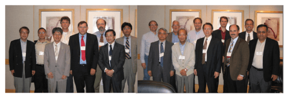
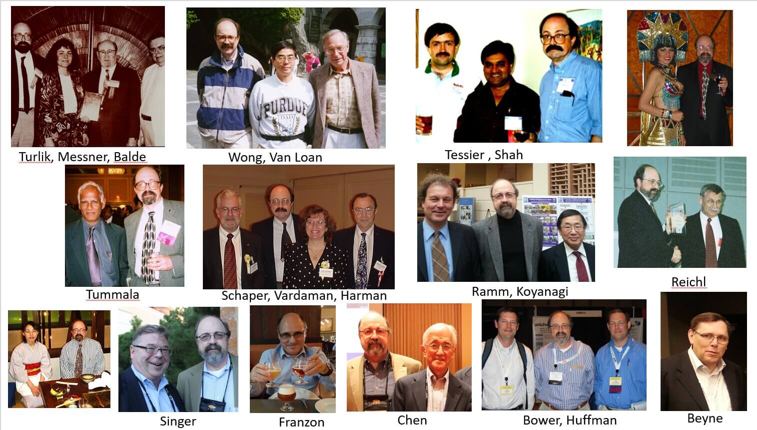
By PFTLE 100 in the fall of 2009 PFTLE was covering the presentations at the first global conference focused on 3DIC sponsored by the IEEE CPMT Society (now the IEEE EPS (Electronics Packaging Society), which Paul Franzon and I chaired. Figure 3 captures the organizing committee, a veritable who’s who for 3DIC in 2009.
A few months later PFTLE introduced the Four Horsemen of 3DIC Integration”: Cost… Test…Thermal Management…Design emphasizing that more was needed than the basic process flow before commercial 3D stacking could be introduced into the mainstream market.

In early 2010, with much of the 3D unit operation processing work behind us, PFTLE began to focus on efforts of standardization, which most agreed had to start with memory stacks.
Then, after 128 weekly blogs, in April of 2010, Reed Elsevier, the owners of SI sold off their magazine portfolio and pulled the plug on Semi International. As the SI web pages were shut down so were the links to all of my work! Lesson for all current and future bloggers …Internet Blogs are not archival!……
IFTLE Begins – 2010
Pete Singer quickly moved over to PennWell publishers and the newly merged (2009) Advanced Packaging / Solid State Technology magazine /web page and brought me with him. There were worries concerning the copyright on “PFTLE”, so I reluctantly changed the title to “Insights from the Leading Edge (IFTLE)” and thus it has remained ever since. In June of 2010 we were back online as IFTLE with the following statement:
 As Jack Nicholson said in the Stephen King classic “The Shining
…………I’m baaack………………
That first IFTLE back in 2010 covered updates from the ECTC conference of that year and an announcement that the IEEE had bought out the EIA and now had full ownership of the ECTC conference. I was especially proud of that last item since I had been working on accomplishing that acquisition for several years during my IEEE Electronic Packaging Society (EPS) [at that time known as CPMT] presidency and that of Bill Chen who followed me.
The relationship with PennWell’s Adanced Packaging/SST franchises worked well for nearly 8 years and 395 IFTLE blogs, but I could see trouble was brewing once again towards the end of this period when contributors’ checks were being delayed for many months at a time. There was always some excuse but the inevitable closure finally came.
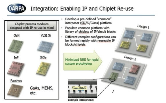
 This time I acted quickly and talked to my old friend, Francoise von Trapp who had established the 3DInCites community back in 2009. Seemed like a good spot to reestablish IFTLE and she was quick to welcome me on board. This time I kept the IFTLE acronym and we started up with number 396 with an update on the DARPA CHIPS program, which had started in 2017, and of which I was a participant. This of course was the precursor to today’s chiplet mania in the advanced packaging community.
Things at 3D InCites for the 100+ blogs have gone as smooth as silk. Thanks to FRT (now Formfactor) who sponsored IFTLE for 2 years, and to our current sponsor, EV Group.
Looking back, there have been several things that I have intentionally tried to do with IFTLE.
The number one premise for this blog has always been to share with our worldwide readership what was being presented at the major and minor conferences held around the world on topics pertaining to Advanced Packaging. There are very few of us who have the budget or time to allow us to personally attend all of these meetings so PFTLE/IFTLE thought we could try to share what went on and get that information back to our readership.
But…instead of covering these meetings the way traditional reporters would with inconsequential comments from authors or titles and a one-line summary, IFTLE selected key presentations and shared the key slides from those presentations. Did I always pick out the most important papers? Who knows…but you certainly got an in-depth look at what I picked out.

Although the front-end IC techies had treated the back-end packaging techies like serfs for the past 50 years, IFTLE tried to make it clear that the packaging community needed to stay up to date on what was going on in the front end or we would be like blind people trying to paint portraits. In that vein, considerable time has been spent looking at what the front end was doing and the impact that could have on the back end.
Similarly, though I am not a design or test expert, I thought it was important to stay on top of the major design and test activities especially as we were trying to bring 3D ICs to commercialization.
From my 25+ years at Dow experience, which ranged from R&D through new product commercialization, I knew how long it took to get new concepts through the pipeline. Thus, while the commercial marketing houses like Yole Developpement were out there proposing rapid market acceptance of advanced packaging like 3D TSV stacking technology, IFTLE was always throwing cold water on such inflated market numbers and short adoption time frames, which in hindsight has been very accurate.
My past experience indicated that a proven concept in R&D usually takes at least a decade to reach its first $1MM in sales. Again, in hindsight, 3D IC has taken even longer than that to gain commercial acceptance because of the enormous changes that were required in the infrastructure and business supply chain.
New things take time to really be understood and adopted, so when IFTLE found a technology that it thought could have a significant impact, we intentionally covered it multiple times to update and for reinforcement. My best example of this would be Ziptronix and its direct bond interconnect (DBI) process.
Ziptronix spun out of Research Triangle Institute in 2001 without a primary application or a customer base. It took them a while to realize that their oxide bonding process had relevance to CMOS image sensors (CIS), but once they did, the industry quickly adopted the technology and ran with it. While Toshiba was the first to adopt it in late 2008, licensee Sony has built their leading CIS market share on these oxide-oxide and copper-copper bonding technologies.
IFTLE has probably covered this technology 10 times or more over the decade. Our interest proved correct as we have recently seen all the major players (TSMC, Intel Samsung, etc.) having what we now call “hybrid bonding” on their roadmaps to replace copper pillar bumps as we moved to ever finer interconnect features. Was the commercial community waiting for the original Ziptronix patents to expire or was this simply a technology ahead of its time? …I’ll let you answer that.
Another technology that IFTLE has highlighted more than a dozen times is micro-transfer printing (MTP). It came out of a college laboratory in Illinois around 2005 as the startup, Semprius. It is basically a massively parallel pick and place technology looking for an application. I worked with Semprius and its CEO Joe Carr (a long-time Dow colleague) in its early days but left when they decided to focus on manufacturing solar panels (IFTLE is NOT a fan of expensive energy sources).
While their solar efforts didn’t succeed, the technology persisted and eventually spun out again as X-display, under Chris Bower, a company using the technology to move massive quantities of tiny LED components to fabricate LED displays. It has also become clear that MTP is also relevant to heterogeneous integration and with the help of X-Fab lives on as X-Celeprint. While MTP has not yet been included on the roadmaps of Intel, Samsung or TSMC just yet, my gut tells me there is something there and it will find larger applicability… eventually.
So what do I think have been some of the technical highlights that IFTLE has covered in the last decade?
General Observations:
- #1 is obviously watching packaging evolve from an afterthought to the important position that it now holds in the overall industry.
- IFTLE has enjoyed watching longtime colleague Rao Tummala and his GaTech packaging center brethren bring microelectronic packaging into the educational mainstream
- IFTLE has watched ASE’s Bill Chen pour his heart and soul into the Heterogeneous Integration Roadmap. That kind of commitment is rare and should be applauded.
- IFTLE loved watching Peter Ramm and Mitsumasa Koyanagi get the credit they deserved for being pioneers in the development of 3DIC integration.
- IFTLE has watched Eric Beyne from his early days as a grad student to his current status as a worldwide leader in advanced packaging.
- IFTLE is thankful for having had the opportunity to have worked with advanced packaging colleagues like Jack Balde, George Messner, Avi Bar Cohen, Iwona Turlik, George Harman, Ted Tessier, Pete Elenius, Herb Reichl, Jan Vardaman, Paul Franzon, CP Wong, Len Schaper, Eric Beyne, Michael Toepper, Paul Van Loan, Pete Singer, Peter Ramm, Mitsu Koyanagi, Bill Chen and so many, many more.
- IFTLE also thanks Alan Huffman and Chris Bower whom he has tried to mentor through the years. It might be arrogant to call them protégés, but I’ll do that anyway!
- Consolidation is a natural occurrence in all manufacturing genres. In the last decade, consolidation has occurred throughout the advanced packaging supply chain.
- This was evidenced by watching front-end equipment suppliers, AMAT, TEL, LAM buying up smaller back-end packaging equipment suppliers.
- Watching the IC community attempt to move to 450mm and fail and watching Moore’s law and scaling slow down has reinforced the old saying that “all things must come to an eventual conclusion”.
- The 2014 sale of IBMs NY fabs to GlobalFoundries summoned the end of IBM as we knew it.
- In 2009 I predicted to a group of Government agencies that IBM would soon be out of the IC fabrication business due to the evolving economies of IC fabrication. I was laughed off the stage then…but who got the last laugh?
- Would any of us have ever predicted the demise of DEC, Motorola, IBM, NEC, Hitachi, or Fujitsu as IC giants?
- IFTLE has been fascinated by buzzword evolution whether it be “multichip modules” or “internet of things” or “wafer-level fan-out” or “nanotechnology” or “3DIC” or most recently “chiplets”. Especially watching all the secondary and tertiary players in the ecosystem trying to develop their “spin” to attempt to sell their technology as fitting into distorted definitions of these buzz words.
- In fact what I have seen over the years is that the bigger the technology’s ultimate success, the more naysayers there were initially predicting those developments would never happen. Specifically, I can call out: Bumping, wafer-level packaging, hybrid bonding, chiplets, and oh so many more. Those entrenched in the old classical technologies say “Never going to happen” but technologies that serve a need can never be kept down for long.
Specific Technology Predictions:
- Although fan-out WLP was a natural evolution for WLP, who in 2006 would have predicted that Infineon and its e-WLB process would win out over Freescale and its RCP (redistributed chip package)? e-WLB licensing to ST Micro, ASE, StatsChipPAC, and many others settled that question
- A plethora of technical issues evolved as the community attempted to commercialize 3DIC such as:
- Eric Beyne’s IMEC group solving the copper extrusion issue
- Brewer Science developing numerous new products to meet the evolving requirements of 3DIC temporary bonding
- In the early days of 3DIC, it was unclear who would own the processes to create TSVs. The more we learned about “vias middle” technology the clearer it became that TSV were meant to be introduced front end in the fab and not back-end in the assembly houses
- Watching Qualcomm, at one point the strongest corporate advocate for 3DIC in the world, ( Matt Nowak, Riko Radojcic, Liam Madden, Steve Bezuk) pulling the plug a bit too early on their 3D efforts was unfortunate, but expected when a company enters a technology too early and has to carry those costs over an extended period of time
- While Micron and its hybrid memory cube (HMC) consortium got all the early hype, it was Hynix who took HBM over the finish line to become today’s gold standard in stacked memory. (Samsung and Micron belatedly followed.)
- The amazing work that Doug Yu and his team at TSMC have done on advanced packaging (CoWoS; InFO; SoIC)
- Xilinx 2011 introduction of Vertex-7 FPGAs using disintegration and silicon interposers (Suresh Ramalingam et. al.) as the forerunner to today’s chiplet technology.
- Amkor’s mainstreaming of copper pillar bump technology
- 3DIC stacking becoming the main technology for advanced CMOS Image sensors mainly due to the technology of Ziptronix and the outstanding development work of Sony
- Bryan Black coming out at the GaTech Interposer Tech workshop in 2011 and stating that AMD was moving to 2.5D and stacked memory approach…our first exposure to what we now call chiplet technology
- Industry confusion over the definition of “3DIC integration” and then even more confusion (extending to this day) over the definition of chiplet technology
- Watching typically front-end processes such as lithography and CMP become standard packaging tools. Today’s advanced packaging house must have this capability in their repertoire if they are doing advanced packaging
- IFTLE is amazed that while the use of metal lead frames and wire bonding has become passe, mold compound has managed to maintain its position in today’s leading packaging applications
- Watching the reemergence of what we used to be called “large-area processing” into “panel-level processing”
- Watching the transformation of multichip module technology, MCM, of the 1990s into the system in package, SiP, the technology of the 2000’s
- Watching Ho-Ming Tong coin the phrase “ 2.5D” in 2009 saying that ASE was not quite ready for 3D. What was initially a joke became a standard genre of advanced packaging.
- Watching Corning, Schott and Asahi Glass try to bring glass substrates into the mainstream of IC packaging. It has not happened yet…but maybe it will.
- Watching traditional underfill evolve into NCP and NCF
- Watching transfer molding evolve into compression molding.
- As we move to more and more modular partitioning, watching warpage become one of the most important things to control in advanced packaging.
I could go on forever, but I won’t…you get the big picture.
What started with Bob Nowak and Don Dix of Dow Chemical saying to me in the mid-1980’s “Your job is to get us into materials for microelectronics” created a career path for me that has allowed me, at this point, to share my thoughts with the worldwide packaging community. What more could a techie ask for?
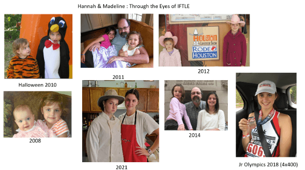
A review of IFTLE 500 would not be complete without mentioning that being “old school” and proudly never ever having been accused of being “politically correct” I don’t do social media. You will never find me on Facebook or Twitter. My only dabbling in “sharing” personal info, however, has been sharing a pictorial history of my granddaughters growing up with my PFTLE/IFTLE readers (Yes I know …that’s what grandparents do!)
My first picture of Hannah and her little sister Madeline appeared in 2008. The readers’ favorite photo was Halloween 2010. Hannah is now 5’11”, medaled in the 2018 Jr Olympics in the 4×400, and is equally academically accomplished. She will be heading off to college next fall with Madeline following a few years behind. When I am gone, I’m assured that they will carry on admirably.
Lastly, I don’t exactly recall when the editorial advisors of Advanced Packaging were assigned caricature photos but when I saw mine, I loved it and henceforth have used it for all matters private and public. Hannah and Maddie call it “cartoon grandpa” It’s kind of a reverse of the “portrait of Dorian Gray” theme. While I get old and wrinkly, the caricature does not. This certainly is the way I want to be remembered.
 So, as Bob Hope used to say “Thanks for the memories”.
Here’s to IFTLE 500. I don’t know how many more will come. I’m now well past retirement age but why retire when you’re still having fun!


