
Heterogeneous Integration spurs demand for 3D backend solutions
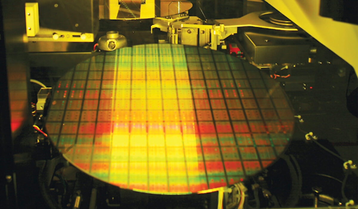
Julian Ho reported in the Jan 10th issue of Digitimes that heterogeneous integration of diverse semiconductor components to support 5G, AI, automotive electronics, and IoT applications is gaining significant momentum, driving demand for system-in-package (SiP) and system-on-3D package (So3D) processes and boosting the importance of chip probing and system level test services. They report that in order to extend its packaging technology lead over Samsung Electronics and Intel, TSMC will enter volume production of its 4th generation chip-on-wafer-on-substrate (CoWoS) packaging in 2019, and its 5th gen CoWoS will be available in 2020 to package high-performance computing (HPC)) chips needed for artificial intelligence (AI). Mainly applied to package GPU and FPGA chips, CoWoS has helped TSMC land orders for HPC chips from Nvidia, AMD, Xilinx, HiSilicon, Google and others.
Besides 4th generation, CoWoS, InFo WLP, and fan-in WLP, TSMC’s wafer level system integration (WLSI) platform has also incorporated more advanced system-on-integrated-chips (SoIC) and 3D wafer-on-wafer (WoW) package solutions.
Samsung FOPLP
As we have discussed previously [see IFTLE 389, “Samsung 2μm L/S Panel Level Packaging Technology Revealed at ECTC “] the Samsung Packaging Development Team presented a paper entitled “Fan Out Panel Level Package with Fine Pitch Pattern” discussing the technical challenges of fine pitch processing on a panel level process.
Digitimes also discusses the status of fan out panel level packaging (FOPLP). According to Ho, Samsung Electronics is the most aggressive in developing FOPLP technology. Ho reports that Samsung FOPLP is still in early stage development and that reaching economies of scale will be a major challenge as current yields are not good enough to develop cost-effective FOPLP production capacity in the short term. Currently, Samsung can only apply the technology for relatively low-end applications. Initially, FOPLP has only been applied to processor power management ICs for Samsung’s new wearable watch.
Apparently, the FOPLP technology is too immature for packaging high-performance chips such as AI chips, GPUs, ASICs, and FPGAs. FOPLP process equipment also entails significant investment risks, as existing panel or foundry equipment cannot support FOPLP production and heavy investment is required for new equipment installation. Powertech Technology has begun construction of FOPLP packaging lines in Hsinchu at a total cost of $1.62B with startup set for the second half of 2020.
ASE Technology Holding is also getting prepared for volume FOPLP production, which reportedly could begin in mid-2019 at the earliest. ASE has set panel specs at 300x300mm and 600x600mm to package high-end chips, including datacenter server chips, FPGA chips, GPU chips, and network communication processor chips.
EPTC 2018
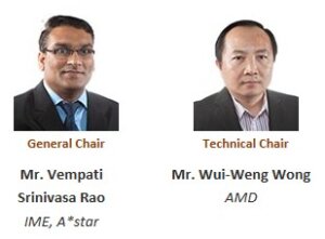 The 20th annual Electronic Packaging Technology Conference ( EPTC) was held in Singapore in early December 2018. The General Chair was VS Rao of IME A star and the Tech Chair was WW Wong of AMD (Figure 1).
Over 190 technical papers and 20 invited presentations were presented in 35 oral sessions and two poster sessions. Key topics included:
- TSV/Wafer Level Packaging
- Interconnection Technologies
- Emerging Technologies
- Materials and Processing
- Equipment and Process Automation
- Electrical Simulations & Characterization
- Mechanical Modeling & Simulation
- Thermal Characterization & Cooling Solutions
- Quality
- Reliability & Failure Analysis
Let’s take a look at some of the more interesting papers that were presented at this year’s conference.
Fudan University
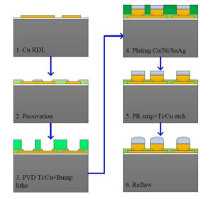
Researchers at Fudan University. in China discussed “…the effect of bonding properties of micro bumps for different morphology and interconnection methods”. They compared the bonding of copper pillar bumps (CPB) of different exterior morphology with different bonding methods. Their CPB process flow is shown in figure 2.
To study the effect of bonding properties for different morphology of micro bumps and different chip-to-chip bonding methods, they fabricated CPB where the tin cap was reflowed and compared it to CPB where the tin cap was not reflowed and the tin cap remained flat. They then compared the bonding by reflow and thermos-compression bonding (TCB).

According to their experimental results for flip-chip (FC) reflow, when the top and bottom chips are interconnected by using reflow and non-reflow copper pillar bumps, respectively, there will be neither obvious shifting nor large voids in the bonding interface. However, for the TCB method, it is difficult to control the bonding profile for small CPB because small changes in pressure, temperature or time, may cause great changes in bonding profile.
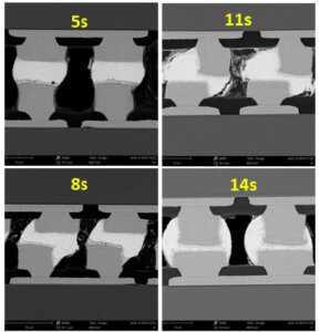
For example, Figure 3 shows TCB results when the temperature and pressure remain the same (300 C and 30 Newton, respectively ) and the bond time is changed, i.e. 5 seconds, 8 seconds, 11sec and 14 seconds.
Whether the pressure is increased or the time is increased, the result is that the two copper pillars are very close and the solder is squeezed out from between the copper pillar bumps.
Huazhong University of Science & Technology (HUST)
J Li and co-workers discussed “Low-temperature Cu-Cu bonding by self-reduction of particle-free Ag ion paste”. In this work, a low-temperature Cu-Cu bonding method is described through the reduction of an Ag citrate paste. The paste was uniformly coated as a bonding interlayer. After exposure to 200 °C and 1 MPa for 10 min, the Ag paste was reduced to Ag metal, and a Cu-Ag-Cu interconnect was formed. This interface could achieve shear strength over 20 MPa. They propose application in high-power electronic device packaging.
Fujifilm – New Temporary Bonding Materials
Fujifilm and STATSChipPAC discussed “Temporary Bonding Material Study for Room Temperature Mechanical Debonding with eWLB”. Temporary bonding materials (TBM) are widely used in TSV technologies, wafer thinning and backside redistribution layer (RDL) process in various kinds of 2.5D and 3D IC manufacturing. Various kinds of debonding methods are utilized, including thermal release, solvent removal, laser assisted, and mechanical debonding. Most current temporary bonding/debonding materials required release layers that are either laser sensitive for laser-irradiation release and/or adhesion control between glue and substrate boundary. This release layer may cause a defect issue after debonding and may cause difficulty with cleaning and ashing of the carrier wafer and device rework process. Fujifilm report on a newly developed single layer TBM having no release layer for room temperature mechanical debonding. Strangely, they give no name for this new material making one wonder if it is a real product at this point. Their material shows no significant weight loss after 4 hours at 230° C. After separation, the residual TMB is removed from the wafer using a solvent. Subsequent solder ball shear test indicated that Cu pads were cleaned effectively after the temporary bonding and debonding process.
For all the latest in Advanced Packaging stay linked to IFLE……………………………….


