

TSMC recently held its 26th annual Technology Symposium, so let’s take a look at the highlights of their presentations focusing on their advanced packaging activities featuring a new concept called 3D fabric.
But first, among the front-end highlights were the following:
- Scaling from the N7 to N5 to N3 process node proceeds on an aggressive schedule
- N7 entered high volume manufacturing (HVM) in 2018, at Fab 15.
- TSMC provided a forecast for more than 200 N7/N7+ new tape-outs in 2020.
- N5 started HVM in 2Q2020, at Fab 18 in Tainan.
- N3 is defined, electronic design automation (EDA) vendors are in active development and HVM is planned for 2H22.
- N3 will utilize a traditional FinFET device architecture.
- While FinFET devices offer significant performance improvements over planar devices, one disadvantage is the additional parasitic capacitance.
- TSMC announced that they will be introducing an air-gap process in the dielectric between gate and source/drain to reduce these parasitic.
- TSMC is planning a huge R&D investment for technology development past N3.
TSMC’s 3D Fabric
- Chip-on-wafer-on-substrate (CoWoS), integrated fan-out (InFO), and system-on-integrated chip (SoIC) are being grouped under a “3D Fabric” product umbrella in anticipation of future mixing of these three technologies in the same system-level assemblies
- CoWoS (2.5D) technology is expanded to include a local silicon interconnect (LSI) bridge, embedded in an organic laminate (similar to EMIB) called CoWoS – L. The company sees CoWoS as offering a useful and cost-effective solution for the integration of multiple dies with memory stacks.
- InFO (2.5D) technology now has a similar option of using an embed silicon interconnect bridge. This will be known as InFO-L.
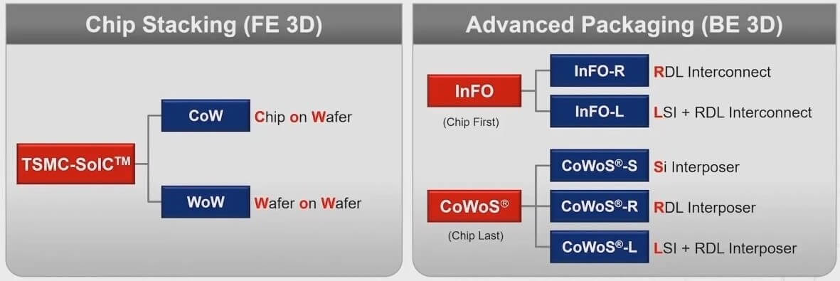
SoIC
As we have discussed recently (see IFTLE 457, “Hybrid Bonding Coming of Age” ) TSMC’s hybrid bonding solution called SoIC enables thermo-compression bonding die. This technology is capable of 0.9um pitch. TSMC indicated that bond and through silicon via (TSV) pitches will indeed transition from 9µm (N7) to 6µm (N5) and to 4.5µm (N3). They shared data on sub-um bond pitch reliability, for such future node scaling.
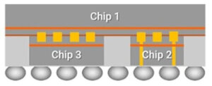
Both face-to-face and face-to-back orientations are supported. The face-to-back topology utilizes TSVs to provide the bonding pads. TSVs can also enable the addition of micro-bumps for subsequent package substrate attach (Figure 2).
In the specific case where both dies have the same footprint, bonding can be done wafer-on wafer or WoW. This is commonly used to construct high-bandwidth memory (HBM) stacks, with several memory die on top of a memory controller as the base. A 12-high HBM stack (total thickness ~600µm), utilizing the SoIC bonding technology has been proven.
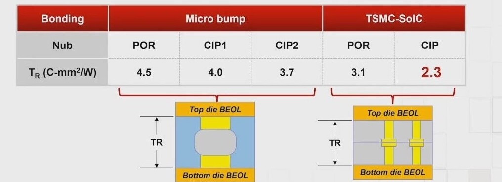
TSMC has also shown how their hybrid bonds thermally outperform micro-bumps as shown in Figure 3.
CoWoS
Their first advanced packaging technology commercialized about a decade ago, CoWoS is shown in Figure 4.
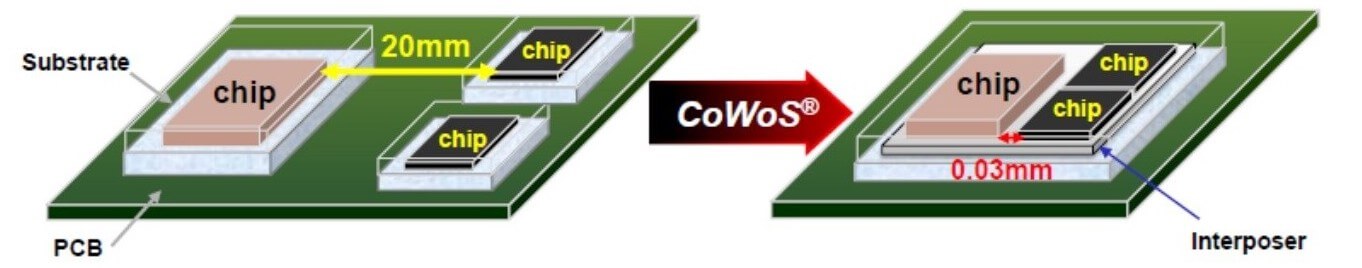
CoWoS has traditionally used a high-density silicon interposer as the interconnect substrate for multi-die integration. This option has been the mainstay for system implementations with an array of processor die, typically with HBM memory stacks as shown in Figure 5.
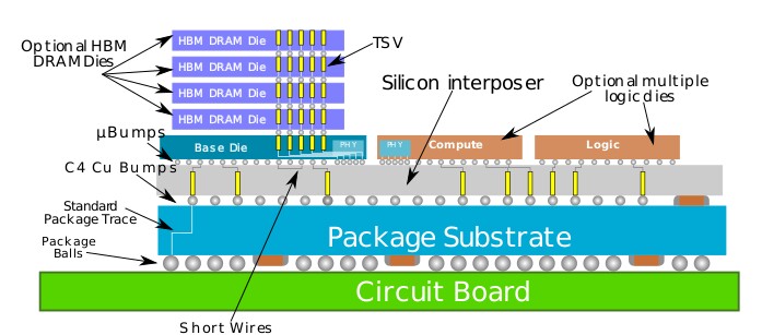
TSMC will be expanding the interposer size to 3X max reticle (2021) and 4X max reticle (2023), to support model processors and HBM stacks in the overall package.
CoWoS process developments now enable:
- Up to 5 Cu metal layers
- 3X lower sheet resistivity (1H21)
- Embedded capacitors
The traditional CoWoS architecture with silicon interposer is henceforth designated as CoWoS-S vs the introduction of the new CoWoS – L
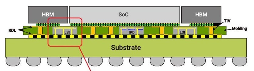
CoWoS-L
The silicon interposer is replaced by an organic substrate with an embedded silicon bridge interconnect (LSI), reportedly offering interposer-like interconnect signal density in a more cost-effective assembly (Figure 6).

InFO
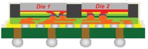
TSMC’s InFO was introduced a few years ago. It was a major breakthrough for fan-out advanced packaging when it was inserted into the iPhone. InFO encapsulates KGD face up on a “reconstituted” wafer, places copper pillar bumps onto the I/O, molds and planarizes them. Then they build RDL on these wafers and bump them resulting in structures as shown in Figure 7.
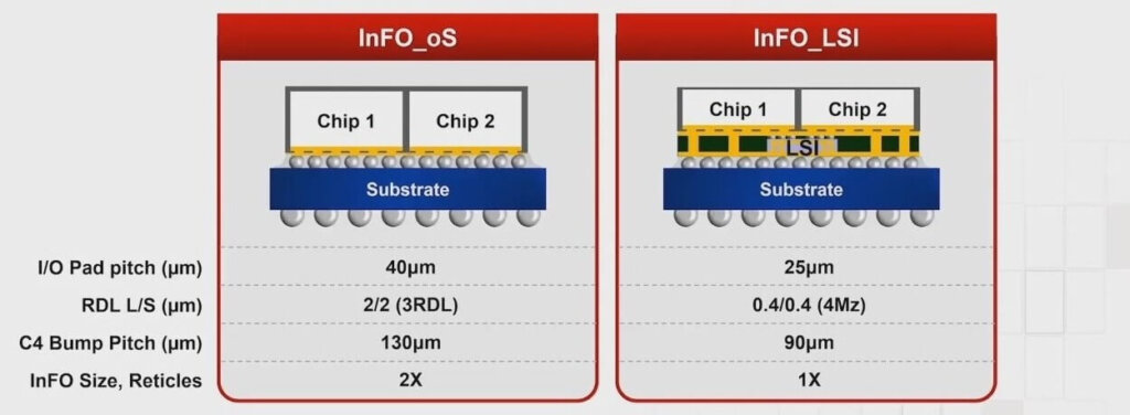
TSMC is now introducing alternative InFO technologies. The traditional InFO assembly with redistribution layers is now being called InFO-R. Design parameters include 40µm pad pitch; 2µm L/S and 3 RDL layers. Support for an InFO 1.7X reticle-size assembly will be available in 4Q20, with 2.5X in 1Q21 [1X reticle size ~33mm x 26mm]
InFO-L
As with the CoWoS technology, InFO is now offered with a laminate substrate and an LSI bridge for high-density connection.
Compared to the baseline InFO-R technology, the embedded silicon bridge in InFO-L offers a tighter die pad pitch, smaller L/S. They expect to be qualified in 1Q21 (Figure 8).
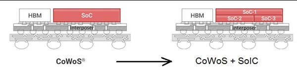
3D Fabric Mixed Technology Integration
TSMC envisions a combination of (SoIC + InFO) and/or (SoIC + CoWoS) assemblies. The example below shows how SoIC can be integrated as part of a CoWoS assembly (Figure 9).
According to Focus Taiwan, TSMC is in the process of preparing for a new high-end integrated circuit packaging and testing plant scheduled to start operation in 2021. TSMC already operates advanced IC packaging and testing plants in Taoyuan, Hsinchu, Taichung, and Tainan.
TSMC will reportedly invest US$10.11B to build the new IC packaging and testing plant, the largest ever single investment in the county, in the Chunan area of Hsinchu Science Park. It is scheduled to be completed in May 2021, with operation starting in mid-2021,
For all the latest in Advanced Packaging stay linked to IFTLE………………………..


