
I first started covering Ziptronix and its hybrid bonding technology back in 2007 when I was writing Perspectives from the Leading Edge (PFTLE) for Semiconductor International (SI). I’d give you the references, but SI went belly up in 2010 and I learned my first lesson about the NON-archival nature of the internet as my 100 plus blogs all disappeared one Friday night as they closed down.
I had moved my Dow offices into the Microelectronics Center of NC (MCNC) which was later acquired by RTI International. RTI spun off Ziptronix and its patented wafer bonding technologies in 2000. At that point, Ziptronix was a technology in search of an application. Remarkably, the company survived a full decade as a startup before its breakthrough in 2010, when Sony licensed their Zibond technology for CMOS image sensor (CIS) applications. As usually happens when a technology has merit, all the other CIS manufacturers soon followed (OmniVision, Samsung, etc.).
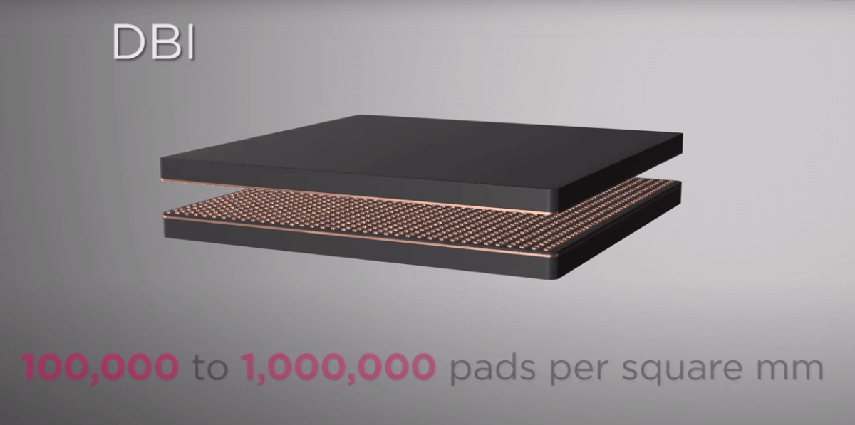
In the fall of 2016, Invensas (then part of Tessera and now Xperi) acquired Ziptronix for $39MM and began its quest to expand what was then a wafer-to-wafer (W2W) hybrid bonding technology called DBI™ to a die-to-wafer technology (D2W) technology now called Ultra DBI™, in order to broaden its application space.
Die-to-Wafer Stacking with Low Temp Hybrid Bonding
Xperi, in its presentation “ Die-to-Wafer Stacking with Low Temp Hybrid Bonding” at this summer’s virtual IEEE ECTC Conference, continued to detail the development of the DBI Ultra process.
Most practitioners agree that to achieve bump pitch beyond 35µm, we will probably require a direct Cu-Cu bonding technology (not copper pillar bumps). Such direct Cu-to-Cu bonding can be achieved through two means: Cu-to-Cu thermal compression bonding, or room temperature hybrid bonding.
Xperi reports that the advantages of DBI over compression bonding include:
- Superior control of the Cu pad coplanarity through CMP
- Room temperature bonding with no need for vacuum or inert environment
- Fast bonding cycle time due to the spontaneous nature of the initial oxide-to-oxide bonding
- No need for external pressure during bonding or anneal
- Fully sealed Cu pads during anneal, with no oxidation concern
- Low anneal temperature with no need for metal barrier coatings on the Cu pads
- Hermetic seal of the Cu interconnect for the high-reliability in-service environment.
In fact, all commercial products using wafer-to-wafer hybrid bonding to achieve direct Cu-Cu interconnect are using the DBI technology, i.e. CMOS image sensor and 3D NAND memory.
While W2W DBI bonding is well suited for certain applications with matching die size on both wafers and high die yield on each wafer, D2W DBI bonding (DBI Ultra) opens up a much wider application space. Thus, Xperi wants to apply DBI Ultra to applications such as DRAM high bandwidth memory (HBM) stacking and memory-on-logic products for high-performance computing (HPC). The company is also looking at redesigning system-on-chip (SoC) to 3D chips ala chiplet technology.
DBI Process Flow Review
IFTLE has gone over the DBI process flow many times in the last 10 years. But…for any newcomers here it is again(Figure 1).
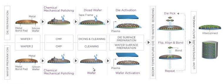
Dicing is a dirty process so the diced chips must be thoroughly cleaned and then plasma-activated. Bonding is carried out in a pick and place flip chip bonder. Once the full wafer is populated with die, it is put into an oven and during the heating, the copper expands to react with the bottom pad and form a monolithic copper joint. Controlling surface topography is critical to process success.
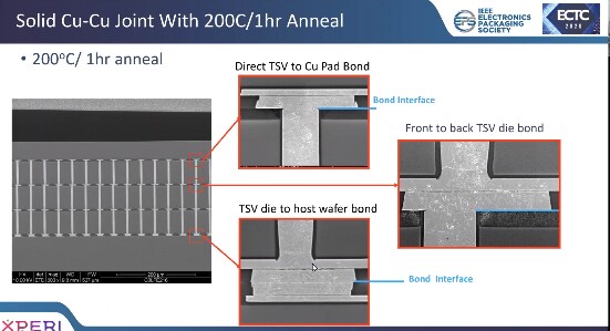
Die stacking as would be required for HBM is shown in Figure 2 for 8 x 12 mm 50um thick die with 5µm TSV on 35µm pitch.
Invensas published a D2W stacking process at ECTC in 2018 and integrated TSV into DBI Ultra in 2019. Oxide bonding of multiple layers takes place in an ambient environment. Once all layers are placed, the host wafer goes through a batch anneal. Cu-Cu connection through all bonding interfaces forms in the single batch anneal.

In mid-July, Laura Mirkarimi, Xperi’s VP of 3D portfolio, gave an IMAPS webinar entitled “Hybrid Bonding: Fueling Advanced Memory and High-Performance Compute Roadmaps”.

According to Mirkarimi, current licensees of the technology include:
- Fraunhofer (ASSID), Sandia, SRI
- Sony, OmniVision, and Samsung (in the CMOS Image Sensor application space)
- Nhanced Semi, Teledyne Dalsa, Qualcomm, Raytheon, Tower Jazz, UMC, and SK Hynix.
IFTLE feels pretty confident that the Hynix agreement, announced in Feb of this year, is focused on HBM memory stacking and attempting to reduce the cost of such stacked memory products. When asked whether the Samsung license allowed them to develop memory products, Mirakami’s response was a simple “Yes”.
IFTLE wonders whether Micron is considering these developments. Micron has been playing catch-up in the stacked memory application space since its failure to bring its “hybrid memory cube” technology to high volume manufacturing.
Xperi claims licensee UMC is actively scaling up the hybrid bonding technology, though not quite ready to accept customer orders. UMC and Tower Jazz would be strong sources for fabless players to gain access to the technology.
While TSMC has never (to my knowledge) used the term “hybrid bonding” let alone DBI, IFTLE has thought its SoIC technology certainly looked like hybrid bonding (see below).
During the IMAPS webinar, Mirkarimi was asked about TSMC and their SoIC technology and responded that “…it appears to be fundamentally the same”.
It certainly looks like Hybrid bonding “has come of age”.
For all the latest in Advanced Packaging stay linked to IFTLE……………………………. ~ Phil


Comments are closed.