
Continuing our look at the hybrid bonding (HB) presentations at the recent IMAPS Device Packaging Conference with a look at Adeia’s presentation. Adeia (previously known as Xperi/Tessera/Ziptronix – Tessera acquired Ziptronix in 2010) has been focusing on bringing die-to-wafer (D2W) HB to the memory market. The presentation discussed “Hybrid Bonding Interconnect and Advanced Packaging Solutions” and detailed some significant data on HB technology as developed by Adeia.
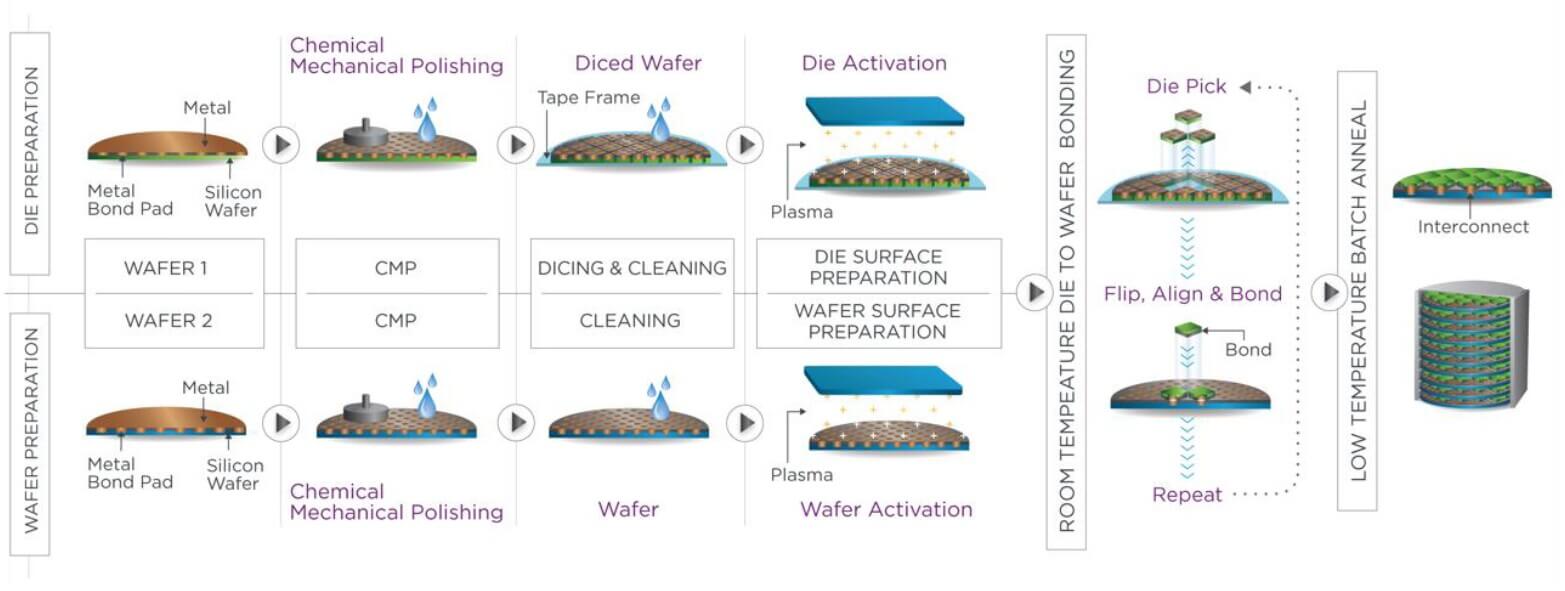
The Adeia die-to-wafer process flow is shown in Figure 1:
They list the following as criteria for high volume manufacturing (HVM) D2W Hybrid bonding (HB):
- Robust nanoscale CMP:
- Smooth dielectric with recessed metal bond pads
- Tight control of mean metal recess depth
- Minimal within wafer and within die recess variation
- HVM processing for dicing through bonding:
- Clean environment
- Saw, stealth laser, or plasma dicing depending on the device
- Dicing and post-dicing processing on a tape frame
- The process needs to be compatible with long queue times (i.e. weeks)
- Pick & place bonder design must be compatible with HB:
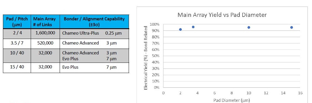
- Alignment accuracy suitable for device pad/pitch (3 sigma < 0.25x pad size)
- Bonding environment and robotic motions compatible with particle control down to 0.2um
- Anneal
- Fully bonded interfaces at anneal temps of 200°C.
Adeia’s test vehicles show no significant drop in yield for pad sizes down to 2µm (Figure 2)
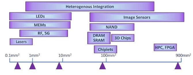
Typical die sizes vs. application space are shown in Figure 3.
There is no decrease in yield for thinner die (50µm) vs thicker die (200µm)
For 8 x 12mm die (50µm thick) with 15µm bond pads:
- D2W electrical yields are > 99% down to ~75µm from
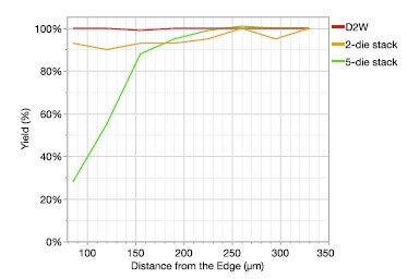
- For die stacks yield loss extends farther from edge (200um) as stack height increases (Figure 4).
For a 12-die stack of 8 x 12mm (50µm thick) die with 15µm bond pads, the overall yield was 56% with an average per layer yield of 95%.

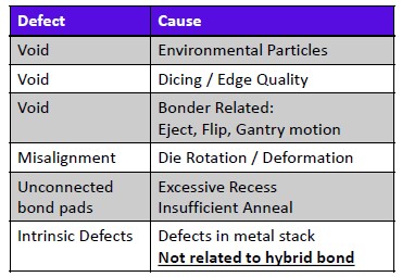
Failure Analysis:
E-test failures are examined by CSAM, IR microscopy, and SEM cross-section
- 99% of electrical yield loss is correlated to voiding
- Voids are randomly distributed within the wafer
- Voids more prone to be in edges and corners
- The vast majority of voids have detectable particles (5-50µm) at the void center
Table 1 lists potential sources of yield loss:
Reliability Testing
The results of reliability testing are shown in Table 2: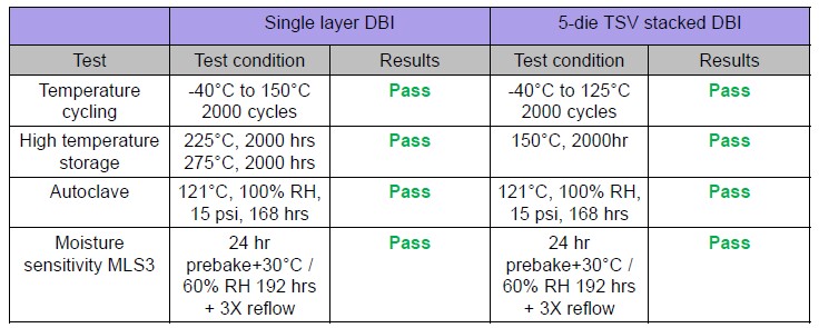
For all the latest in advanced packaging technology stay linked to IFTLE…………………


