
Sorry for the disruption of the chronological flow of my recent blogs, but before I move on to the July coverage of the much-anticipated IMAPS “ONSHORING” conference, I wanted to continue covering a few of the papers from the 2023 IMAPS Device Packaging Workshop, which took place in March.
As longtime readers of IFTLE know, we have been tracking the commercialization of “hybrid bonding” since it was first discussed and patented by Paul Enquist and his colleagues at Ziptronix in the early 2000s. It has emerged more than two decades later (Yes truly new technologies sometimes take a decade or more to catch on) as a key technology in high-density packaging such as 3D IC.
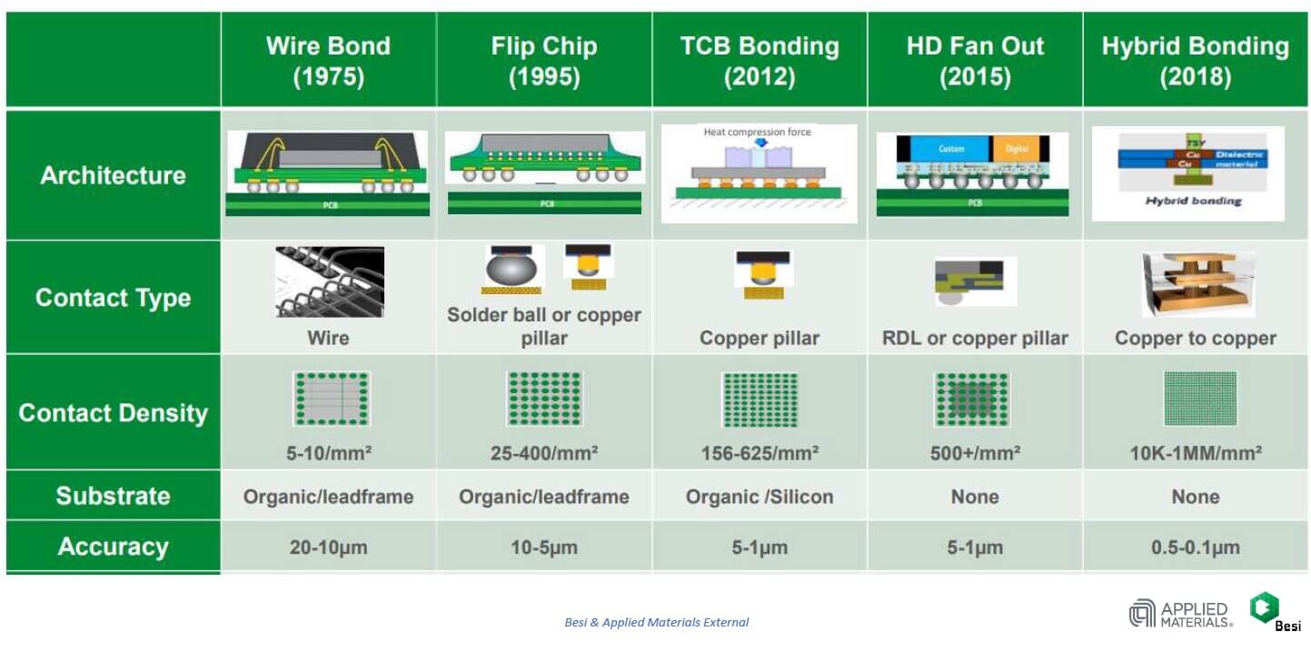
Hybrid bonding (HB) involves simultaneous metal and dielectric bonding. It provides both mechanical support and dense electrical interconnects between vertically bonded chips. Cu is the commonly used interconnect. It has been the driving force for the miniaturization of CMOS image sensors and is currently being evaluated in 3D memory stacking including 3D NAND and SRAM. All the major packaging players such as TSMC, Intel, and Samsung have it on their process technology roadmaps (Figure 1).
By the way, I’ve said it before and will continue to say, “It’s about time that one of the major packaging societies like IEEE EPS and/or IMAPS gave Enquist and his Ziptronix team (now Adeia) one of their technical achievement awards. I think having your technology show up on Intel, Samsung, and TSMC roadmaps is justification enough…Don’t you??
Anyway, its now common knowledge that “hybrid bonding” (HB) is becoming an integral part of our advanced packaging toolbox.
Besi and HB
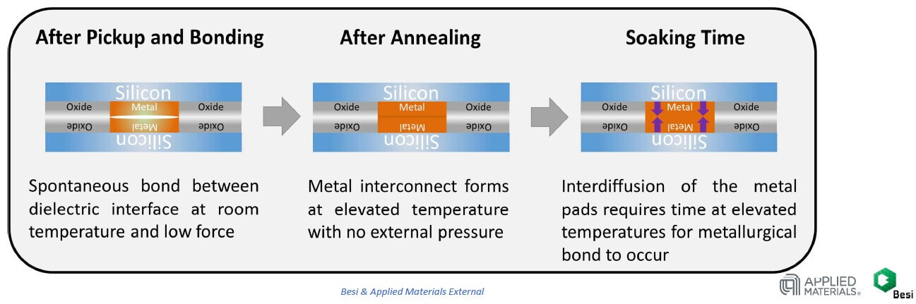
The BESI presentation “Chip-to-Wafer Hybrid Bonding Development for High Volume Manufacturing” focused on BESI and Applied Materials (AMAT) declaration that hybrid bonding is the next-generation bonding technology (Figure 2).
The rest of the presentation addressed HB challenges, and BESI / AMAT proposed solutions.
- CMP dishing: Ensure proper thin barrier thickness and that barrier height is lower than SiOx profile.
- Cleanliness: Any particle on the bonding surface can lead to poor adhesion, weak bonding, or complete bond failure. This is a challenge for diced wafers on flex tape since the dicing process can introduce part
- Plasma activation: Bonding degrades with excessive time between activation and bonding. Also, when the plasma ion energy is too high the surface is roughened creating voids, which degrades the bonding.
The Chameo 8800 is Besi’schip to wafer bonder. They claim it is the first high volume die to wafer hybrid bonder (in production since 2022). They also claim it has 200µm placement accuracy (with 100µm in development and a roadmap to 50µm). It can place 2000 chips per hour and is designed for die pick up from a film frame / So/glass carrier.

EV Group and HB
The EVG presentation focused on “D2W Hybrid Bonding using High Accuracy Carrier Solutions for 3D System Integration” First EVG compared W2W and D2W HB (Figure 3).
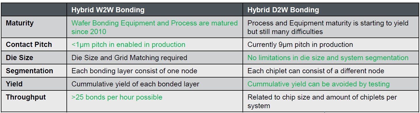
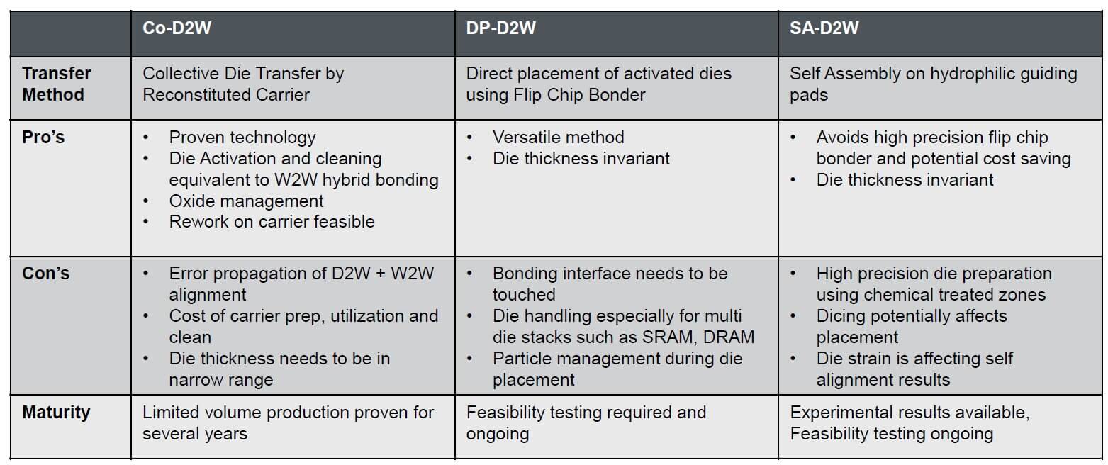
Figure 4 shows EVG’s recently announced die-transfer technologies.
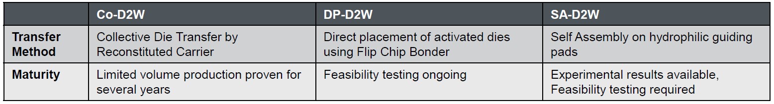
EVG assessment of these options is shown in Figure 5:
For all the latest on advanced packaging stay linked to IFTLE………………….
For more on Hybrid Bonding, listen to the latest episode of the 3D InCites Podcast.

