
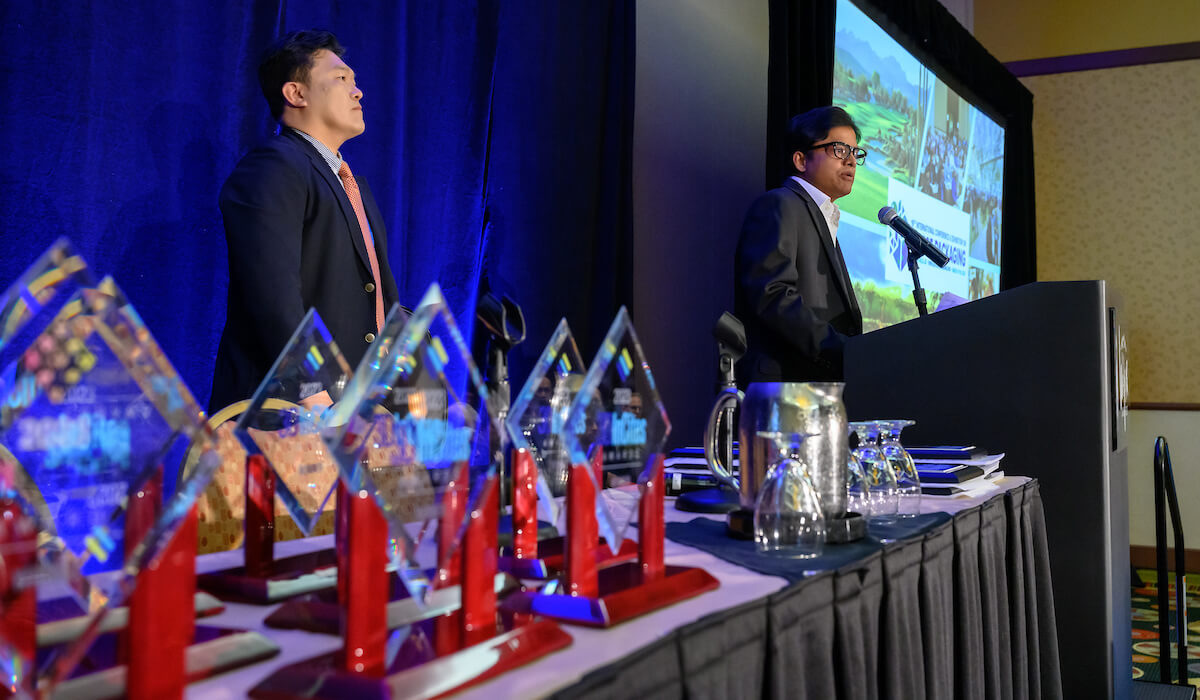
What an energizing week I had at IMAPS DPC 2023! I’ve said it before, but it’s worth saying again, the IMAPS Device Packaging Conference (IMAPS DPC) is one of my favorite annual events, and this year’s edition did not disappoint. There was a record turnout, great keynote talks, panel discussions, networking opportunities, lots of new technology developments, and of course, key industry players exhibiting their latest processes, technologies, and products. We were there for it all, as the official podcast of IMAPS DPC. Over the next few weeks, we’ll be “dropping” some great episodes (that’s podcast-speak for broadcasting).
More and more, it’s becoming clear that how we interconnect and protect semiconductor chips is critical to the future of semiconductor technology. At IMAPS DPC 2023, the messages rang loud and clear: We need chiplets, we need advanced fan-out, and we need high volume advanced packaging capabilities in the US.
IMAPS DPC 2023 Focused on Chiplets
Ahmer Syed, Qualcomm Technologies, Inc. kicked off the event with a keynote on the topic, Challenges for the Next Generation of Package Technology and Integration. I am always interested to hear Qualcomm’s position on this topic because as a fabless company, they tend to be a barometer for which of the latest and greatest technologies will be adopted. If you recall, after investing in the development of 3D integration technologies, including through silicon vias, Qualcomm ultimately killed its program, opting for a fan-out wafer-level packaging approach that was more cost-effective.
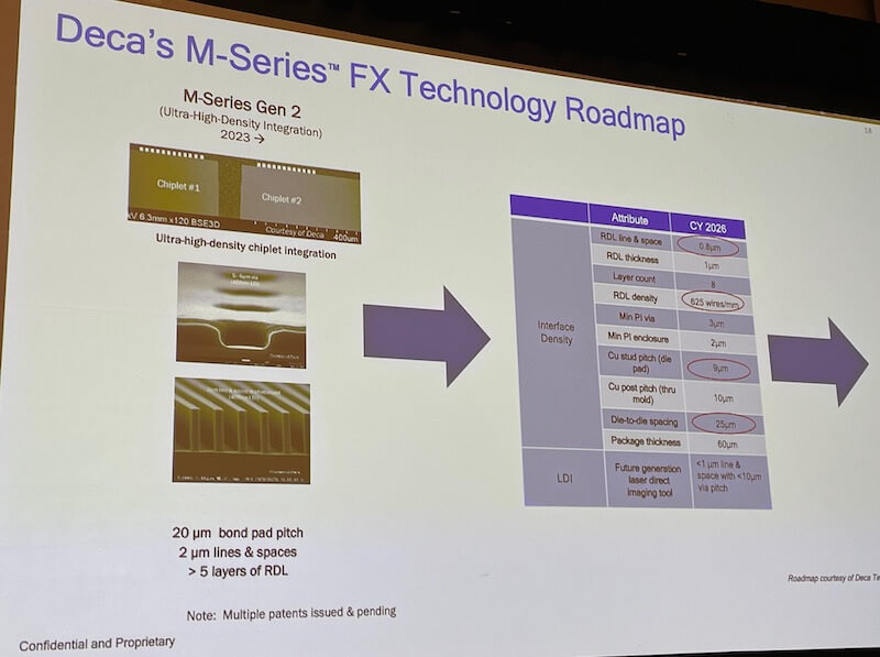
It seems the company hasn’t changed its approach. Syed described two tiers of packaging technology integration as options. One is chiplet integration, a function of design that disaggregates systems on chips (SOCs) into its functional blocks, so that each can be built at the most optimal technology node and reintegrated using advanced interconnect technologies – namely hybrid bonding. The second innovation he mentioned was advanced RDL technology for advanced fan-out packaging. Syed cited the next generation of Deca’s M-Series (he called it M-Series FX), in which the RDLs become part of the chip (Figure 1). I look forward to hearing more about that from the team at Deca.
As per usual, the end application will drive which packaging solution is adopted. Syed noted challenges driving innovation included new failure modes impacting advanced materials, such as coefficient of thermal expansion (CTE) mismatch. He did say assembly processes need to move towards fab-like tools, advanced processes, and automation to ensure high yields.
When asked by Jan Vardaman whether Qualcomm is considering hybrid bonding and stacking memory on top of that as an option, he responded that it would be considered if the density requirement increased enough. Currently, Qualcomm is still using thermocompression Cu bonding.
When asked about whether Qualcomm would purchase third-party chiplets, Syed responded that it depends on the final application. “For premium tier mobile or compute applications, I prefer to keep things in my control, versus using third party chip(let)s.” he said.
Given all the discussion around the importance of building a high-volume advanced packaging house in the US, Jan also asked if such a place existed in North America, would Qualcomm use it? Syed responded, “That depends on the business model.” Over the years, I’ve come to understand what this response really means – “if it’s cheap enough!” Rather, Syed envisioned technology being developed in the US and assembled in an offshore location. Sound familiar? All food for thought.
The Harbinger for Chiplets
On the flip side, Samsung’s SW Yoon talked about the need for chiplets to provide the high-performance computing needed for artificial intelligence (AI), and to support the massive data explosion it is creating. As many others have noted in the past few years, Yoon pointed out that Gordon Moore had a second law. If you read further in his famous paper, he notes that “It may prove to be more economical to build large systems out of smaller functions, which are separately packaged and interconnected.” This has become the harbinger for chiplets.
Yoon noted that Samsung sees the cost advantages of chiplets when compared with SoC. “No longer is shrinkage the answer. No single process is fit for all,” he said.
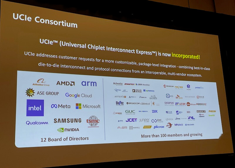
Up until now, chiplet integration has only existed in vertically integrated companies such as Intel and AMD. Broadening its application will require some standardization on the interface used for interconnecting chiplets. As such, Yoon announced the official incorporation of the Universal Chiplet Interconnect Express (UCIe). Samsung is one of 12 companies with a seat on UCIe’s board of directors (Figure 3).
In other areas of advanced packaging innovation, Yoon announced that Samsung introduced an industry first: fan-out wafer level packaging (FOWLP) stack technology replacing flip chips and a silicon interposer in graphics memory packaging.
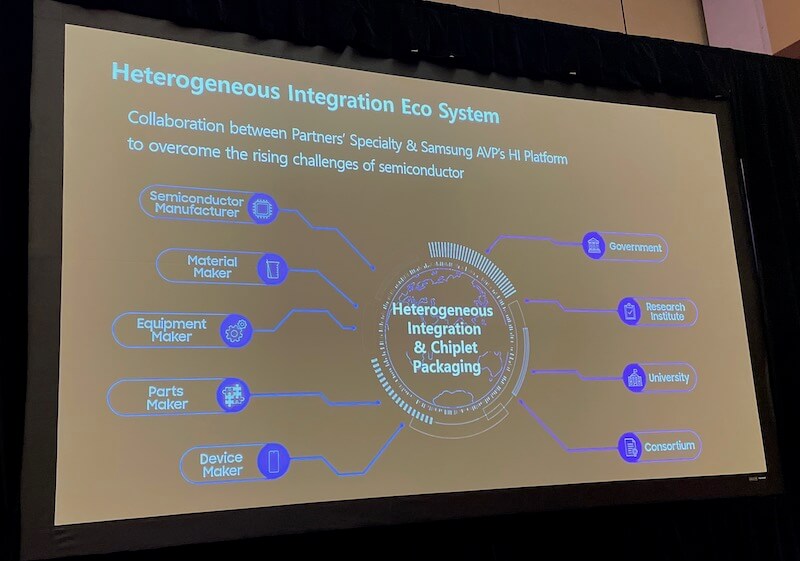
Lastly, Yoon talked about Samsung’s establishment of a Heterogeneous Integration Eco System, a collaboration between partners’ specialty and Samsung Advanced Packaging HI platform to overcome the rising semiconductor challenges (Figure 4).

Chiplet Panel Demystifies Chiplet Challenges
The chiplet conversation continued with the Tuesday evening panel, organized and led by Jan Vardaman. She rounded up at least one representative from each part of the supply chain to provide different perspectives on chiplet challenges including:
- Lihong Cao, ASE Group | Sr. Director Engineering and Technical Marketing
- SP Jeng, TSMC | Director, Advanced Packaging Technology & Service Group
- Mike Kelly, Amkor Technology | VP, Advanced Packaging Development and Integration
- Choon Lee, JCET Group | Chief Technology Officer
- Ravi Mahajan, Intel Corp. | Intel Fellow
- Chris Scanlan, Besi Switzerland AG | Senior Vice President Technology
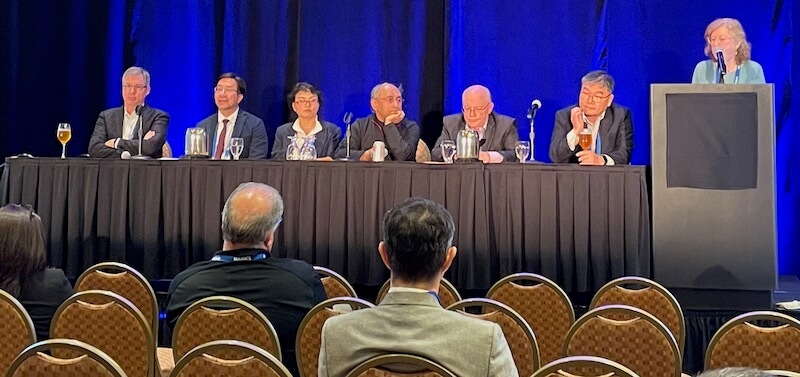
What ensued was a lively discussion that served to illustrate the complexities of chiplet integration.
Chris Scanlon described the chiplet “problem” as an “interconnect problem” saying that “The most advanced interconnect technology in our toolbox is hybrid bonding – but we can’t use it for everything – and not everything requires it.” He also reminded us that chiplets are not a packaging technology and shouldn’t be confused as such. He said he thinks about it like this:
- A multichip module (MCM) is a way to package things that never got around to being an SoC.
- A system-in-package (SiP) connects things that could never be packaged on the same chip.
- Cbiplets are integrating things that used to be on a SOC but aren’t anymore.
The question of when 3rd party chiplets will come into play was the most controversial. Because chiplet integration is a function of design, how can we be sure that third-party chiplets will work when they are connected? As John Hunt noted, alluding to the focus of the UCIe: “if you’re using different die from different foundries, just because the interface is standardized, doesn’t mean chip performance will be standardized.”
Then there is the question of hybrid bonding, which is essentially a front-end process. For OSATs to adopt it, they must invest in clean room space and equipment. All the OSAT representatives agreed, that if there was enough customer demand for Cu hybrid bonding, they would make the investment.
SP Jeng emphasized that for TSMC, its chiplet product – SoiC – is front-end oriented. He said chiplets provide savings over SoC, and as such doesn’t really see it as something that will make sense for OSATS. Ravi Mahajan disagreed, saying that for Intel, it’s a matter of both technical and economic sense, and he sees a point in time where OSATS will have a role to play in chiplets.
And then came the question from Doug LaTulipe, of Draper Labs, which sent me back a few years to the days of similar discussions around the adoption of TSVs – if we use third-party chiplets and assemble them at the OSATS – who owns the problems? Nobody really had an answer for that – but Choon Lee did note that it took 10 years for TSVs to come to the OSATs, so perhaps we’ve got a little time. I do recall that what ended up happening in the case of TSVs, was that whoever’s name was imprinted on the final package, owned the challenges. So, I guess that’s another topic for another day.
And this was just what happened on Tuesday!
The DEI panel, the path from research to industry, packaging for today’s automotive electronics, photonics packaging…
There was a lot going on! But we captured conversations from all of these activities in the 3D InCites Podcast – so stay tuned for upcoming episodes.


