
I wanted this blog to cover the recent whitepaper by Siemens’ EDA division on chiplet model standardization, and it will, but first I need to go over some introductory material on chiplets, and specifically, chiplet definition. Let me explain why.
As part of the work that I do with the government. I have been helping ascertain onshore microelectronic advanced packaging capabilities at:
- U.S. IC fabricators
- U.S. assembly/packaging houses,
- Defense industrial base (DIB) companies.
While those overall results remain proprietary of the government, I can tell you that my biggest surprise was the number of companies (mainly in categories 2 and 3) that were not clear on the meaning of chiplets. Many of the companies responded that they were fabricating chiplet modules in the US, which on further questioning turned out to be simple multichip modules (MCMs) or standard systems-in-package (SiPs).
When you realize that I was talking to supposed senior professionals in packaging, (not MBAs), this result was a bit shocking. One giveaway was when I asked what communication protocol was being used for chiplet communication in the modules, and the response was “I don’t know what you mean.”
Anyhow, it became clear that the chiplet definition needs to be reviewed until it is understood by everyone. For those of you who feel this is a waste of your time because you are already educated, my apologies.
Chiplet Definition
So… let’s review the official definition of “chiplet” by the Electronic Packaging Society (IEEE EPS*)
“The naming of new technologies can be difficult and often inaccurate. Over time, standards are developed and language becomes aligned.
The cost of leading-edge nodes, combined with the lack of scaling of significant design blocks (ex: analog) and die sizes reaching reticle size, is driving disaggregation (splitting up) of chip functions into their best price/performance nodes requiring new technologies to interconnect these functions.
We are voicing our support in naming these small IP blocks “chiplets”. It is not a perfect name but fits into our vernacular well and is gaining acceptance in our industry. Our definition of “chiplet”, and what it is not, follow.
Chiplet is not a package type, it is part of a packaging architecture. Thus, in large and complex chip designs the design is subdivided into functional circuit blocks, often reusable IP blocks, called “chiplets”, that are manufactured and recombined on high-density interconnect.
Historically the need for multiple chips to deliver a specific function was driven by the reticle limit which dictated the maximum size of a chip possible to be fabricated. Designs that exceeded the reticle limit were split up into smaller dies to be manufacturable. As technology continued to enable increased integration, multiple dies were merged into single, more complex ICs. Thus, the origin of the term “system-on-a-chip” or SoC.
More recently, economics has caused a reversal of that trend. As the industry moves to smaller process nodes, costs for yielding large dies increases. The desire to move to a chiplet-based design has been driven by the increasing cost of manufacturing devices on leading-edge process nodes. Compared to a 250 mm² die fabricated on a 45nm process, a 16nm process more than doubles the cost/mm², and a 7nm process further doubles that to 4x the cost per yielded mm². Moving to the 5nm and even 3nm nodes, is expected to make this even worse.
The chiplet solution can be used to ease the economics of manufacturing such chips, with large numbers of transistors, at state-of-the-art nodes. In chiplet-based design, the chip is broken down, by function, into multiple smaller chiplets and only the chiplets that require the latest node are made in that node.
Some envision, that in time, the greater use of chiplets will drive the package to become the new SoC, and chiplets become the new “IP”. However, for this to be viable across packaging companies, there must be standard/common communication interfaces between chiplets. There are several solutions today, but standards must be chosen.”
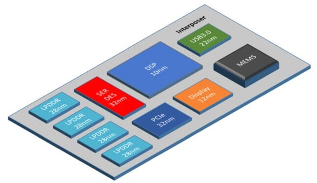
Thus, chiplets are an alternative design methodology to monolithic chips. A single chiplet design would typically have a single function, be operationally dependent on other chiplets, and be reusable across a range of products and product generations. An example is shown in the image above. (Chiplet-based system using an interposer – Source: Cadence)
A major benefit of chiplets over monolithic designs is that smaller chips are significantly more efficient to manufacture (higher yielding). However, one of the fundamental disadvantages is the need for additional on-package interconnects to allow the chiplets to communicate with each other. This extra interconnect can increase the amount of silicon by 10% over a monolithic design. So, while there are definite benefits of cutting up a large chip into many smaller chips, this has to be balanced against the additional costs of the extra area taken up by the interconnects and extra packaging costs.
AMD and Apple both have processors with chiplets on the market and in production in high volumes. This means that: (1) sufficient production capacity has now been built upon the manufacturer side and (2) even large and complex chiplet structures can be designed reliably and manufactured.
The Need for Chiplet Models
Members of the Chiplet Design Exchange (CDX) [ a working group under the Open Domain-Specific Architecture (ODSA) sub-project under the direction of the Open Compute Project Foundation (OCP) ] are proposing a set of standardized chiplet models that include thermal, physical, mechanical, IO, behavioral, power, signal and power integrity, electrical properties, and test models, as well as documentation to facilitate the integration of the chiplets into a design. Additionally, they see security traceability assurance as an emerging need to ensure a trusted supply chain and operational security of the chiplets and the resulting packaged devices. It is strongly recommended that these models are electronically readable for use in the design workflows.
So, let’s look at how CDX defines chiplets:
A chiplet can be defined as a die specifically designed and optimized for operation within a package in conjunction with other chiplets. The interfaces used are a main differentiator. A chiplet differs from a conventional die in that a chiplet cannot typically be packaged separately and still operate effectively; whereas a conventional die has powerful enough I/0 drivers to enable signaling over longer electrical distances. Optimizing a chiplet to operate within a package can be summarized according to the following key metrics on the chiplet-to-chiplet interface:
- Energy efficiency (pJ/bit)
- Bandwidth per beachfront (Gbps/mm)
- Area efficiency (Gbps/mm2)
- Latency (ns)
- Communication Reach (mm)
- Input Output Connection Pitch ( m) “
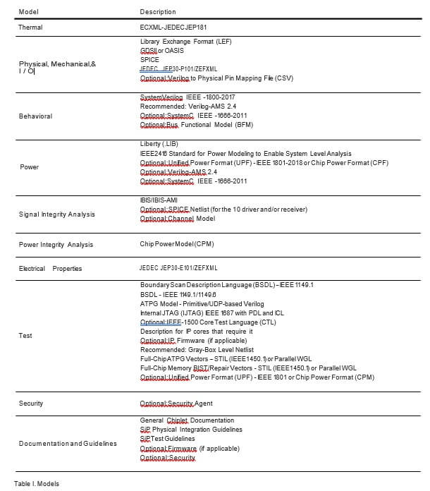
CDX recommends that chiplet providers offering their devices for use in heterogeneous package designs should provide a standardized set of design models to ensure operability in EDA design workflows. CDX proposes a set of standardized chiplet models to be provided by respective chiplet providers. The models should leverage existing industry standards that are readily available, with extensions to these standards and the addition of new standards to be defined as necessary. Table 1 summarizes the proposed chiplet models to enable a usable chiplet ecosystem. Not all chiplets will require all of these models, but there must be a core set of deliverables provided to support design integration, verification, and testing of the chiplet IP into a SiP design.
The white paper details each of the requirements, which I won’t do here, but I recommend you download a copy and read it thoroughly if you are at all interested in ever using chiplets in your products.
An IC datasheet is provided for all ASIC components and generally includes a detailed description of the device, pinout, operating conditions, and electrical/ mechanical specifications. A datasheet should be provided for a chiplet including similar information that would be provided in an ASIC data sheet. Since a chiplet is unpackaged, specific package information would not be applicable. Detailed models should also be provided for the design and assembly of the chiplet into a SiP device, as outlined in the other modeling items included in this section.
Due to the size and complexity of information on datasheets that have to be manually transferred to software tools, they recommend that the data stored in the datasheet be also stored in the JEDEC JEP30 PartModel files, so that consumers can auto-load the relevant data directly into their software tools efficiently and without introducing errors.
Security Guidelines (optional)
Chiplet vendors should provide documentation and guidelines for the hardware and for software integration of security technology to support the end user of the SiP to implement and/or operate security agents, assuring the trusted supply chain traceability of the respective chiplet.
IFTLE has been pointing out for several years that chiplet standardization was necessary…with this document, maybe we are finally getting closer to such a situation.
For all the latest in Advanced Packaging stay linked to IFTLE………………….
*Note… I was part of the technical committee that derived this definition in response to prior confusion in the industry


