
Plasma dicing offers an optimized approach to die singulation as chips get smaller, thinner, and more complex.
As semiconductor content proliferates across networks and devices, there’s a growing demand for increased semiconductor functionality packed into smaller, thinner, and stronger packages. Heterogenous integration is essential to this effort and die-to-wafer (D2W) hybrid bonding has emerged as an innovative approach for achieving complex integrations of multiple interconnected die into a single SoC or chiplet package.
Hybrid bonding creates a permanent bond between heterogeneous die using tiny copper pads as opposed to traditional micro bumps. It enables up to 1,000X greater interconnect density in advanced 3D device stacking while driving signal delay to near-zero levels.
As the pitch narrows between adjacent pads on the die, however, surface cleanliness becomes critical for enabling reliable die-to-wafer hybrid bonding. Any particulate debris or laser damage to the surface may prevent die surfaces from contacting the wafer correctly and result in incomplete bonding.
This challenge invites a fresh look at die singulation methods. Blade/saw and laser-based dicing have served us well and will continue to be the most cost-effective method where the die size is relatively large compared to the width of the saw blade or laser beam, or the wafer has not been thinned making it more susceptible to blade damage at high cutting speeds. For applications where die are very small, and strength and/or cleanliness is critical, plasma dicing is a compelling die singulation approach with several distinct advantages.
Plasma Dicing for Increased Output
Plasma dicing introduces additional key benefits that are now being exploited by early adopters in several volume production applications. Dry plasma etching using a photomask to define the dicing lanes —the space between die reserved for cutting the wafer — supports narrower kerf widths than either blade or laser dicing – which is a major advantage if die size is very small (RFID tags, for example, typically <0.5mm x 0.5mm).
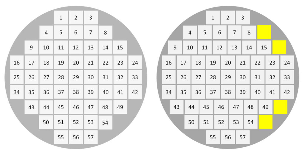
By moving to plasma dicing, valuable wafer real estate is no longer wasted – in fact, it releases wafer space for additional die per wafer, in part because it allows non-linear dicing lanes. Chip manufacturers can effectively increase their output by almost 100% by moving to plasma dicing, depending on the die sizes, when accounting for kerf width reductions and non-linear dicing patterns. This reduces the overall need for additional wafers, process materials, and front-end equipment to increase output (Figure 1)
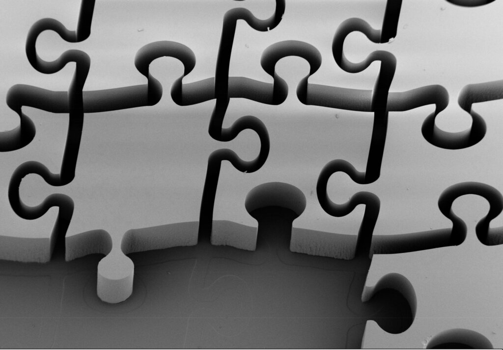
This layout flexibility extends to die shape as well, supporting non-rectangular/irregular shaping, and could accommodate multiple different shapes on a single wafer for multi-project wafers (Figure 2).
Blade dicing and laser dicing are serial processes that cut along the dicing lanes one after the other. For laser dicing, multiple passes may be needed. Plasma dicing removes all the dicing lanes simultaneously. This means as die sizes shrink (i.e., more dicing lanes and therefore more cuts required), and wafers get thinner (less silicon for plasma to remove, or lower blade speeds/ laser powers needed to avoid damage), there’s a clear tipping point whereby plasma dicing becomes the fastest process.

Cleaner Cuts, Stronger Structures
Plasma dicing uses the Bosch silicon etch process whereby silicon reacts with a fluorine-based plasma in the unmasked dicing lanes between chips and is vaporized – like pouring boiling water onto an ice cube. Gaseous by-products are easily removed via vacuum pumping.
This surface cleanliness is critical for emerging hybrid bonding applications, ensuring clean edges around the periphery to eliminate voids in the bond interface. With plasma dicing, there’s no particle or remnant contamination to prevent from making good, clean contact, ensuring the best possible bonding performance.
Unlike with blade and laser dicing approaches, plasma dicing creates no damage at all to the die. There are no internal or surface cracks, heat-affected zones, or chipping to compromise die strength and integrity. This is especially important as thinner die are used to help reduce overall package height when stacked into chiplets.
Plasma dicing is the only valid approach for dicing much thinner wafers, well below 50μm and approaching wafers as thin as 20μm. In a paper published by imec, it was found that it improves die strength more than all other dicing methods tested. This included laser groove (with and without plasma dicing) and laser groove with stealth and blade dicing. Imec concluded that for die-to-wafer bonding, plasma dicing was the better solution for die singulation prior to the bonding stage.
This mechanical integrity gain is an advantage for die subject to physical stresses and strains in service, such as those used in hybrid bonding stacks for high-bandwidth memory (HBM). If one chip in the stack fails, the whole device is lost. Higher break strength minimizes product damage and naturally translates into higher yields.
Plasma dicing is also attractive for fragile devices like MEMS. Inertial sensors consisting of movable microstructures benefit from a clean, non-mechanical singulation method. There are no physical forces to vibrate the wafer and cause damage to the sensing features, or particles to jam in between them, interfering with their movement.
This singulation process is uniquely positioned to enable the adoption and optimization of hybrid bonding, particularly as chips get smaller, thinner, and more complex. Plasma singulation has been proven in high-volume production among early adopters and has even shown promise for non-silicon materials like gallium arsenide (GaAs) and silicon carbide (SiC) in early R&D.
High-density, heterogeneous 3D packages maximize integration. With plasma dicing, the optimizations can begin at singulation.


