
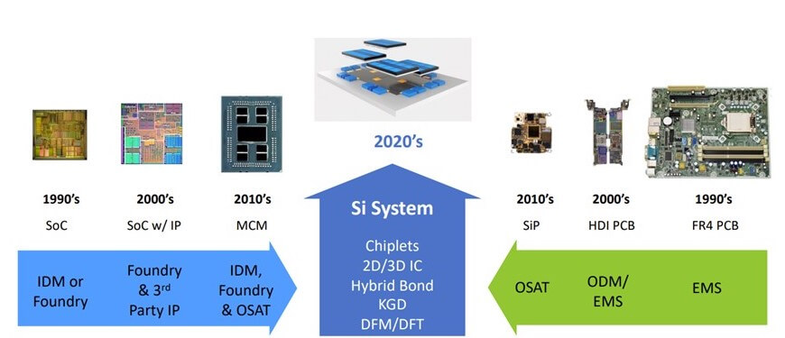
More than a few years ago, somewhere around 28nm, my working group was discussing the potential demise of “Moore’s Law”. The industry and international technology roadmap committee were struggling with hi-k metal gates, strain, FinFETs, and of course how lithography could keep shrinking. The designing and manufacturing of a system on a chip, SoC was becoming extremely challenging and difficult. The packaging expert in the group, Jim Walker, had the answer; the industry would just have to transition to a system in a package or SiP. Walker argued that SiPs would enable the industry to build SoCs in a package. Cheaper, as you were not designing and taping out complex SoC. Faster as you were not designing large SoC and then going through the shuttle process to see if your concept would work. Die size would be smaller so yields would improve. More powerful as you would have more transistors per unit area than you would know what to do with, and time to market would improve. There was the potential for a higher level of profitability.
Fast forward several technology nodes and the concept of SiP has evolved into heterogeneous integration and chiplets, along with a Heterogeneous Integration Roadmap (HIR), and several chiplet standards organizations to help drive the technology along.
There are multiple companies as well as technologies driving 3D packaging. At the recent IMEC ITF world conference, a presenter mentioned that fabless and automotive companies are key drivers of chiplet technology as they are looking at how to combine chips from different manufacturers to meet their specific applications. High-performance computing, with Nvidia, Intel, and AMD as the major players is another high-volume chiplet market, with those three at the forefront of chiplet development. However, when it comes to putting those chiplets together in a package, the focus moves to TSMC, Intel, Samsung, as well as multiple OSATS.
TSMC and Samsung as established foundries are helping their clients put together solutions in a package. Intel is currently using its 3D packaging platform for internal products, but it’s highly likely the industry will see Intel leverage its packaging technology for foundry clients as that part of their business grows.
The 3D packaging is also an alphabet soup of acronyms that sometimes makes sense.
Samsung’s advanced packaging offers I-Cube, H-Cube for 2.5D packaging, and X-Cube for 3D packaging. TSMC with its 3DFabric breaks down into CoWoS (Chip on Wafer on Silicon), InFO (Integrated Fan-Out), and TSMC-SoIC – (Silicon on Integrated Chip). Each of these acronyms can be broken down further as they are used in 2.5D and 3D. Intel might be the simplest with EMIB, 2.5D, and Foveros 3D as its packaging solutions. Not to be left out of the naming, ASE uses a few different terms as well. VIPack then breaks down into a bit more traditional packaging nomenclature. FOPoP, FOCoS, FOCoS-bridge, FOSiP, 2.5-3D, and C0-packaged optics. ASE announce a FoCoS-Bridge at ECTC on May 31. FO stands for “fan out”, a packaging technique that is incorporated in most advanced packages. Each of these offerings combines different methods of putting together the package, which gives the end user multiple solutions to accomplish their products.
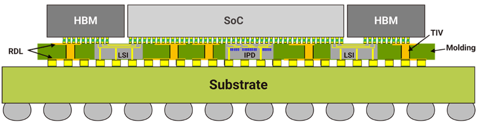
The different names of the 2.5D products give the choices of either an organic polymer where a redistribution layer (RDL) is built up and the chips are connected to each other, or a silicon interposer can be used to make the connection to the other chips in the package or help to define the technology, such as fan-out system in package (FOSiP).
The majority of the 2.5D techniques use some form of bridge to connect the die, either RDL or silicon as discussed above. When using silicon interposers, typically through silicon vias (TSV) are used. Using silicon is more expensive, which is one reason RDL is as popular as it is now. There was significant debate on this topic at IEDM in 2022. RDL techniques appear to use a 2µm line width, and the I/O bumping pitch appears to currently be in the 40µm range across most of the different 2.5D packaging techniques.

3D, or 2.5/3D as ASE and Samsung have put it, typically adds another layer of logic chips to the package. Bridge technology, silicon interposers, and RDL can be used in the same package. The diagrams below by TSMC, and then the Intel example of the Meteor Lake Foveros package, give an idea of the different packaging techniques and their complexity.

The key to shrinking 3D packaging lies in connecting the die to the substrate or interposer. If only bumping is used, there are limitations. The Intel Foveros technology claims they will be at 10µm bumping in 2023. This would be accomplished using embedded bumps. TSMC and Samsung appear to be in the same range. To shrink further, hybrid bonding will be needed. Samsung in their X-Cube literature believes hybrid bonding can get them to a 4um pitch in the near future. This then leads to wafer-to-wafer bonding as well as die-to-wafer bonding, which adds additional complexity.
3D Packaging at imec
At its 2023 ITF world conference, IMEC presented its current work in 3D packaging along with its roadmap showing the future of 3D packaging technology.
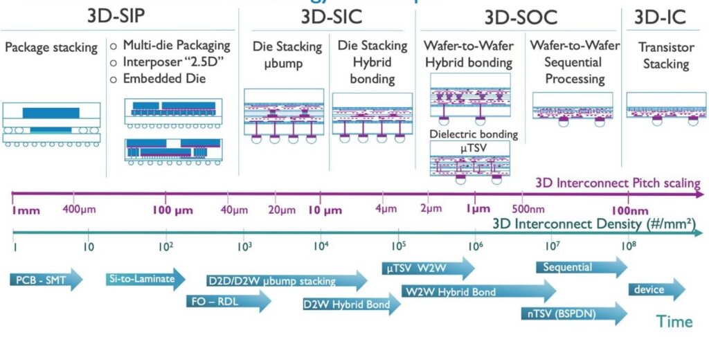
As Samsung and others have alluded, to continue shrinking the package, hybrid bonding will be necessary. Today the industry is looking to introduce 5µm hybrid bonding to complement the embedded bumping. imec’s current work shows 400nm pitch to be possible in the future using hybrid bonding, with the roadmap going to 100nm. If the industry gets there, it will create some amazing SiPs.


