
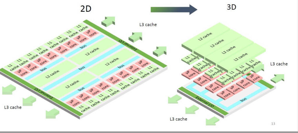
There is a bit of debate about the role that heterogeneous packaging plays in furthering Moore’s Law. Moore’s Law has historically focused on the number of transistors doubling per unit area. In discussions at IEDM, it appears that the definition is being modified to include the chip stacking that is taking place with 3D packaging, where level 1 and 2 memory cache are being stacked on top of the microprocessor cores to improve the memory bandwidth and reduce the energy consumed by the microprocessor accessing the memory (Figure 1). Many years ago, when through silicon vias (TSV) had just emerged, the 3-D transistor stacks were sometimes referred to as Moore’s Law in the third dimension. Anyway, you look at it, the number of transistors per unit area or unit volume is continuing to grow.
A Coming Out Party for 3D Packaging
At IEDM 2022 in San Francisco, there was an increased focus on heterogeneous integration. The tutorials and short courses both had sessions on the topic, and heterogenous integration was one of five focus sessions during the conference.
In a discussion I had with Fabian Clermidy, VP, of Digital Systems and Integrated Circuits Division, CEA-List, we noted that it was the coming out party for 3D packaging. Over the past 10 years, different methods have been experimented with and tried. The current methods being used are a result of those years of experimentation.
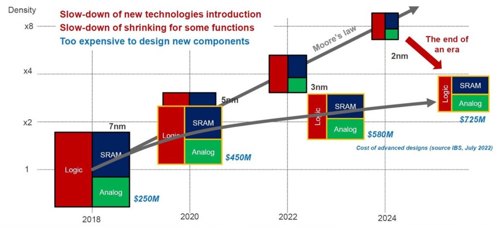
Figure 2 gives a good example of the evolution —or perhaps transition is a better word — from the world of SoC to heterogeneous integration. IP and mask costs continue to rise. Shrinking the transistor and interconnect creates increased manufacturing expenses and chip complexity. Increased wiring generates more heat, which impacts chip performance. Apple’s recent decision to postpone the introduction of their M2 chip demonstrates some of the challenges of designing and manufacturing the next-generation SoC. Heterogeneous packaging enables the development of complex systems in a package that will drive the microelectronics industry forward into the next generation of technology innovations.
Why Heterogeneous Integration?
Heterogenous integration gives designers the ability to create new systems, that with SoC technology would be challenging. The ability to now place different processing chips on the same substrate with accelerators and memory is enabling different types of intelligence for multiple applications. According to Clermidy, some of the challenges include continuing the creation of the 3D eco-system, as well as getting the design IP for 3D packaging a bit further along so more complex systems can be developed.
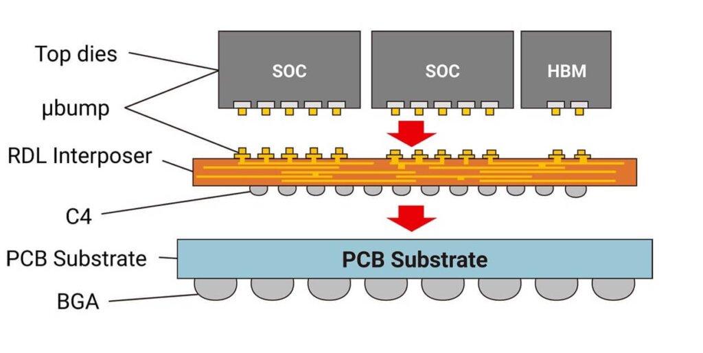
From the IEDM focus session, it appears that the ecosystem is developing nicely. Most of the industry is familiar with the two primary camps for 3D packaging, Intel with the embedded bridge Foveros for 3D packaging, and then TSMC with the 3D Fabric including CoWoS Chip on Wafer on Substrate, with different interposers. At IEDM, TSMC presented its option of an organic interposer using a redistribution layer versus a silicon interposer using TSVs.
The IEDM focus session, Advanced Heterogeneous Integration: Chiplets, and System in Packaging, gave a better insight into other players besides Intel and TSMC working on 3D packaging technologies. ASE, Samsung, AStar, and Unimicron gave their views on the intricacies of 3D integration. One key takeaway was from the Unimicron presentation, where Dr. Lau presented on using an organic RDL layer in place of a silicon layer with TSVs. Lau commented that in Unimicron’s view, the RDL process was more economical and implied that it was potentially more reliable than the silicon interposer. The session demonstrated that several different techniques and substrates can be used for 3D packaging, the one picked for any specific application will depend upon economics, and the reliability needed for that specific application. In addition, the fact there are so many active players means the eco-system is alive and ready for 3D packaging integration.
Challenges and Opportunities for 3D Integration
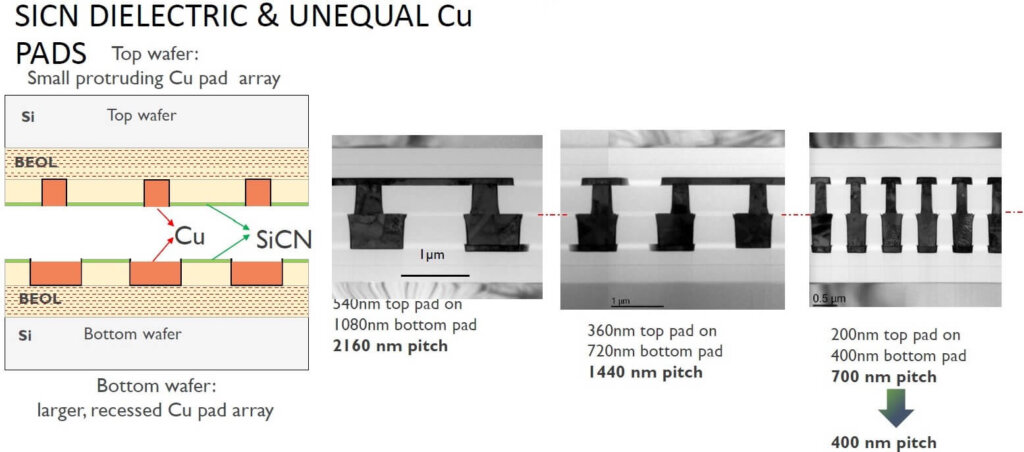
There are still challenges and opportunities ahead in the 3D integration space. As touched on above, fine-tuning interposer technology will continue. Geert Van der Plas of imec pointed out that silicon interposers are expensive, but they work. There are also thermal challenges that have plagued 3D packaging from inception. How to get the heat out will be critical to how densely different chips can be placed together, and then there are also the connectivity challenges: Bumping versus hybrid bonding. To continue shrinking and improving the reliability of 3D packaging, wafer-to-wafer or die-to-wafer bonding will play a key role. Van der Plas, suggests the possibility of achieving a 400nm pitch for wafer-to-wafer bonding in the future, which will continue to shrink the packaging area.

So, while it may not fit the original definition of Moore’s Law transistors per unit area, 3D packaging will continue to enable the increase of transistors per unit volume for some time to come enabling the microelectronics systems of the future.


