


Last year at ECTC 2019, Xperi officially launched DBI Ultra™; the die-to-wafer hybrid bonding version of the highly successful, wafer-to-wafer DBI. Excited to celebrate this momentous occasion with them, I even wore the Xperi logo for the photo. Here we are a year later, and although I won’t have the opportunity to check in with the Xperi team at their ECTC 2020 booth, I was fortunate to catch up with Xperi’s Thomas Workman at the IMAPS Device Packaging Conference 2020 back in March. Workman is the principal integration engineer for DBI Ultra and is part of Laura Mirkirimi’s team of DBI gurus that includes Guilian Gao and Gill Fountain, as well as Gabe Guevara, Cyprian Uzoh, Jeremy Theil, and Dominik Suwito.
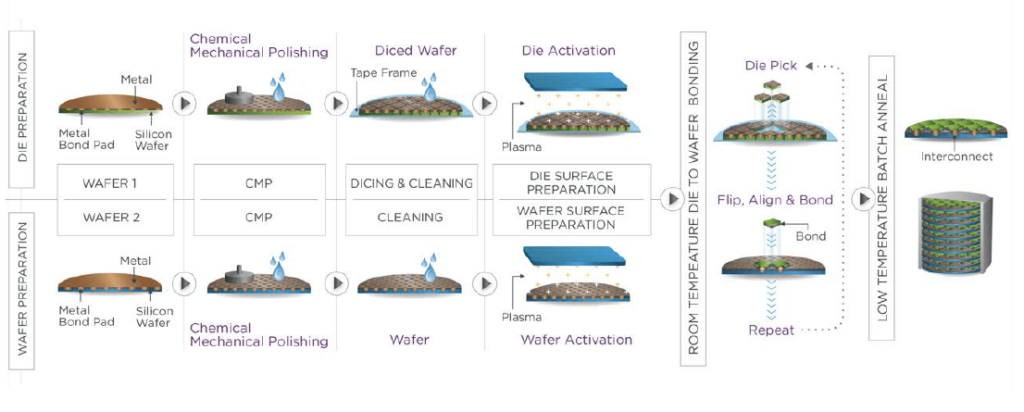
Workman’s presentation focused on how to build the right manufacturing environment to successfully implement DBI Ultra in high volumes. He walked attendees through the DBI back-story: its successful implementation for wafer-to-wafer bonding for CMOS image sensors, and future applications for 3D NAND flash memory. He then went on to discuss the advantages of using DBI Ultra in die-to-wafer stacking applications such as DRAM, 2.5D logic and memory, and ultimately System-on-Chip (SoC) disaggregation ie: chiplet technologies. Figure 2 details the DBI Ultra process flow.
Advantages of DBI Ultra
As a high-volume die-to-wafer bonding solution, Workman provided a laundry list of DBI Ultra advantages over other die-to-wafer bonding approaches including:
- enhanced memory performance
- Improved RLC characteristics
- Superior thermal performance
- Interconnect pitch scales to ~ 1µm
- No added standoff height
- Better overall reliability
- Eliminates organic materials
- Improved Cu-Cu bond
- Potential lower process cost
- Eliminates solder and underfill
- High throughput bonding
- Pathway fewer mask steps
Three Things for DBI Ultra High Volume Success
According to Workman, it all boils down to three critical elements: A robust, nanoscale, chemical mechanical planarization (CMP) process; dicing and handling is compatible with the industry supply chain, and a pick-and-place bonder design that is compatible with hybrid bonding. However, CMP requirements for die-to-wafer are no different than wafer-to-wafer, he explained. So, the team put efforts into validating all major dicing processes – saw, stealth and plasma – and worked with die-bonder suppliers re-design their tools for hybrid bonding applications.
“We don’t want to direct the customer outside their preferred method,” noted Workman. “We always want to be tool agnostic. That is why we are qualifying all dicing methods and die bonders for the process.”
Dicing and Handling
While all three dicing techniques have been demonstrated, Workman says mechanical saw and stealth dicing are most common (Figure 3). However, he says he’s partial to plasma dicing. “Plasma is nice because it’s so clean. You get better edges and can place die close together,” he explained. “However, its more expensive, and requires a mask.”

Ultimately, the dicing process is based on customer preference, so it’s important to understand the advantages and disadvantages of each approach, and how to integrate DBI Ultra into the process flow. For example, Workman said because stealth and saw dicing leave particles behind, it is necessary to have an optimal post-dicing cleaning process. Additionally, the thickness of the die comes into play.
The goal for DBI Ultra is to be compatible with as thin die as possible. So far, the Xperi team has gathered good data for 50µm thick die, but as die thickness changes, so may the calculations. “As die get thinner, they are more susceptible to chipping and cracking. That might inform the choice of dicing,” he said.
DBI’s qualified handling process is die-on-tape, which is the industry standard. Thin die are fragile, but the handling for DBI Ultra is no different than thermocompression bonding, (TCB), noted Workman. “We care more about particulate contamination and need finer control of particles. But we end up with a cleaner process,” he said.
And when it comes to inventory management of wafers post CMP, Workman says there have been no queue issues with either the process flow or storage of the host wafer or die-on-tape.
“The perception is that oxidized copper won’t bond, and so needs inventory management constraints. We’ve looked at this with our CMP wafers. There is no yield loss associated with it; we never found a problem. Wafers can sit in storage longer than a year post CMP. There is also no need to immediately perform the bond immediately after plasma activation. In fact, there is no queue time needed between each step: dicing, post dice clean, activation, and bond.”
The Bonding Tool Environment
DBI Ultra can be performed using a standard flip chip bonder, as long as it has a cleaner environment. Workman recommends a mini-environment (ISO 3 or 4) inside the tool to minimize the remaining particles. The only failure mode is voiding due to particles on the wafer surface.
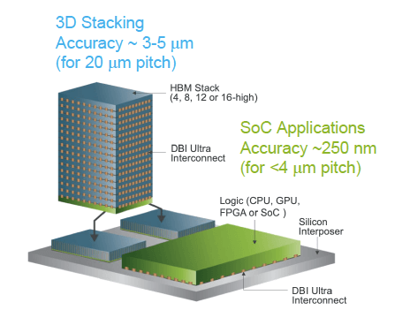
The placement accuracy requirement depends on the application. For example, stacking memory die calls for accuracies of 3-5 mm (for 20 mm pitch), while for SoCs, the alignment accuracy is much tighter- 200-250nm at <4µm pitch (Figure 4). Die bonder equipment is available for memory stacking. Tools for 200-250nm accuracy are in development, and Workman says in house, the team is working with a Besi Chameo fine pitch bonder that is proving to offer better alignment accuracy and cleanliness. They are also in “active discussions” with Kulicke & Soffa, ASM Amicra, and others.

How High Does It Stack?
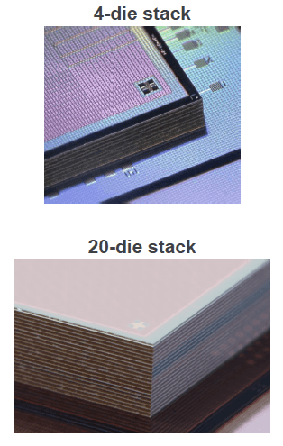
The goal is to achieve constant yield with each layer. Process improvements are increasing the yield at each layer, and so far with four-die stacks, the yield remains constant. How high can we stack it? It seems the sky could be the limit. Workman says 20-die stacks have been demonstrated.
Where Will DBI Ultra Appear First?
Workman predicts the first wave of DBI Ultra will be in memory applications. The company recently signed an agreement with SK Hynix for a technology transfer license. Because memory and image sensors require a looser pitch, existing FC bonders can perform the process, he said.
Through the validation and development process, DBI Ultra also passed automotive reliability testing, which is good news for the plethora of image sensing applications found in automotive electronics.
For more on DBI Ultra implementation in SoC devices, check out this MEPTEC presentation by Xperi’s Javier DeLaCruz. ~ FvT


