
I’ve been following the DBI story for over a decade (well before Xperi became a sponsor of 3D InCites). I’ve watched it grow from its humble, start-up beginnings as a Ziptronix process to its current rock-star status at Xperi/Invensas, as THE current hybrid bonding technology process for image sensors globally. All along the way, I’ve been a diehard fan of this elegant process (AND its entire development team) and believed it to be a game-changer for heterogeneous integration.
So, it is with great excitement, (and a little pride) that I got to take part in the official launch of DBI Ultra during ECTC 2019, in Las Vegas. I even wore an Xperi shirt for the occasion.

DBI Ultra Unveiled
DBI Ultra leverages the same elegant, room-temperature bonding approach as wafer-to-wafer (W2W) DBI, with the added benefit of being both die-to-wafer (D2W) and die-to-die (D2D) processes. This allows for unlimited flexibility for stacking dies of different sizes on wafers of different sizes. It accommodates different process technology nodes and disparate technologies. As such, it is proving to be a game changer for stacking memory die 16 high, as well as 2.5D integration for high-performance computing applications.
I spoke with Laura Mirkarimi, VP 3D Portfolio and Technologies at Xperi, and Guilian Gao, Distinguished Engineer, Xperi, to get the full story.
Blasting Through the Final Roadblock
The only thing keeping DBI from being used across the full spectrum of 2.5D and 3D IC stacking was its limitations as a wafer-to-wafer process. After three years in development, Gao says the technology is now ready to be implemented in die-to-wafer applications.
The paper Gao presented at ECTC, Low-Temperature Cu Interconnect with Chip to Wafer Hybrid Bonding describes how the remaining stumbling block for die-to-wafer DBI has been addressed. While the initial bond is formed at room temperature, until now, high-temperature annealing was necessary to form the Cu-Cu interconnect. Mirkarimi’s team, developed a low-temperature batch anneal process that alleviates the problem.
“Achieving a 200°C Cu anneal is significant,” explained Mirkarimi. “Cu-Cu bonding is usually done at 300°C or higher. Previously, this prevented DBI from being used for stacking temperature sensitive memory devices.” While logic can handle high temperatures, memory and sensor technologies need low-temperature processes.
Hybrid Bonding for the Masses
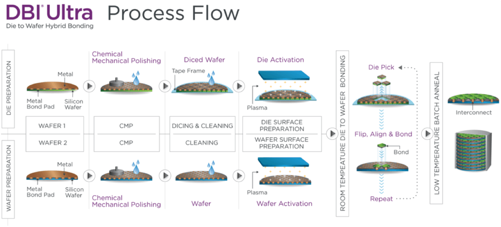
With DBI Ultra, D2W bonding and 3D stacking using TSVs is simple and cost-effective, explained Gao. The foundry prepares the wafers with TSVs and the DBI pad according to design specifications. The wafer is then diced at the outsourced semiconductor assembly and test (OSAT) provider and the known-good-die are stacked on the host wafer or die-to-die, as shown in the process flow in Figure 1.
R&D partners are critical to advancing any disruptive process into HVM. For this project and others, Xperi has relied on the team at Fraunhofer IZM-ASSID for their support.
“We’ve been partners with Fraunhofer IZM-ASSID since 2014,” explained Mirkarimi. “They have exceptional technical capabilities. We value working with Fraunhofer because of their flexibility and willingness to take on new technologies. They are a key part of our supply chain as a 300mm silicon partner and fabricated the wafers with TSVs for this publication.”
Another stumbling block that has been solved was achieving the right die topography to perform the room temperature bond for larger pad sizes. Xperi has developed CMP processes that achieved Cu height variation across the wafer of several nanometers which represents 1000 times improvement over height variation of a micro-bump wafer, explained Mirkarimi.
Nanoscale engineering requires the right tools. We worked closely with atomic force microscopy (AFM) tool vendors to develop procedures for accurate measurement of surface topography to guide CMP process development. “The CMP tools today enable nanoscale engineering and exceptional CMP quality. We are standing on the shoulders of giants and taking packaging into the back-end-of-line, up through CMP and verification,” she said. “OSATs will be able to readily accommodate incoming wafers for stacking and assembly.”
Gao said that being able to connect the TSV directly to the pad eliminates the need for underfill and Cu pillars, creating a thinner profile. “With DBI Ultra, the stack height is the sum of die thickness in the stack and it is possible to stack more die on die, and maintain the same total package height,” she said. “No other technology can do this.”

There are cost advantages to this technology as well, which is important for memory applications, as it can be a cost-sensitive market.
Why is this important? Data centers need more memory, and that is driving memory processor bandwidth, explained Gao. JEDEC wants 12-16 dies in a high-bandwidth memory (HBM) stack but memory stacks must be the same height or lower than the GPU/CPU. Eliminating underfill and bumps enables that. Additionally, an all-copper interconnect provides enhanced reliability, thermal performance, and lower contact resistance.
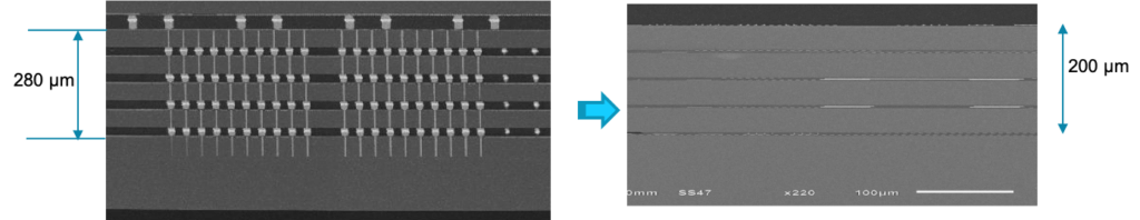
The incumbent technology, thermocompression bonding, requires 240°C reflow, has a 20 µm standoff, suffers from high warpage that leads to yield loss, underfill challenges, and pitch limitations of 40µm. In comparison, DBI Ultra uses a room temperature dielectric bond followed by a final anneal temperature for Cu-Cu interconnect formation around 200C. No underfill or solder interconnect translates to zero standoff (Figure 2). Low warpage in the final product improves yield. Best of all, the process is scalable to ultra-fine pitches down to 1µm.
“DBI Ultra overcomes some limitations in W2W DBI bonding or stacking when the yield in the wafer is low, or the die are different sizes,” explained Mirkarimi. “D2W can be a more pervasive technology. It can be used in high volume manufacturing to stack memory, and also integrate that memory with sensors and logic in a 2.5D or 3D system-in-package (SiP).”
Endless Possibilities
It seems that DBI Ultra is truly unlocking the power of heterogeneous integration. It is ideal for integrating chiplets, a disaggregated chipset that allows for distributed computing. It also enables a more pervasive packaging approach for edge computing. By eliminating solder on both sides of the memory die used in HBM, as well as underfill, it saves, rather than adds, cost.
According to Mirkarimi, DBI Ultra is ready for licensing to begin the transition and ramp to high volume production. By working closely with customers in a technology transfer, Xperi can accelerate product development and integration in a high-volume manufacturing environment.
“We don’t see any major roadblocks and expect DBI Ultra will be in products within the next few years,” she said.
As we’ve said many times before on 3D InCites, before any disruptive technology is adopted there needs to be a big enough problem in the industry for people to take the leap of faith. At this point, with the sensational need for computing, the time to leap is now. ~ FvT

