

Requirements for interconnect pitches of 20µm and below is expected to be the norm in the future. Since typical solder bump technology is not expected to be able to meet those requirements, many companies have been examining Cu-to-Cu direct bonding. Cu-to-Cu bonding can be achieved through one of two ways:
- Cu-to-Cu thermal compression bonding
- low-temperature direct bond interconnect, commonly referred to as “hybrid bonding”.
Thermocompression bonding
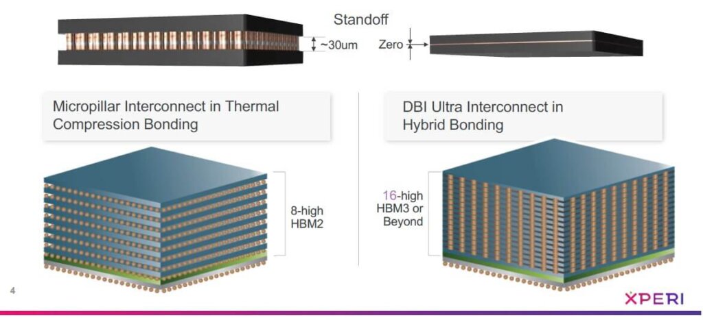
In Cu thermal compression bonding, Cu pillars protrude from the dielectric surface. The pads on the opposite side of the device, paired to be bonded, are held at high temperature (normally 350-400°C) and high pressure to drive the diffusion of Cu atoms across the interface to form monolithic copper. For applications such as DRAM packaging, the process temperature needs to be under 250°C to avoid degrading the device performance. Much of the research in low-temperature Cu-to-Cu bonding has been focused on modification of the Cu surface to achieve bonding temperature reduction.
Copper pillar solder bonding of today’s HBM is compared to DBI™ bonding in Figure 1;
IFTLE has been covering DBI since IFTLE was PFTLE (the predecessor to IFTLE in the now-defunct Semiconductor International: PFTLE 7 – “In Boston, it is called Scrod”), when Ziptronix was spun out of RTI International in 2001, for a wafer bonding technology looking for a commercial application.
In DBI technology, metal pads are slightly recessed from the surrounding oxide dielectric surface. One first forms an oxide-oxide bond at room temperature and then establishes the Cu-Cu bond through a batch anneal at 150–300°C. Since the initial oxide bonding takes place at room temperature, Cu oxidation during bonding is minimized. The bonded oxide layer surrounding the Cu interconnect protects the interconnect from oxidation in the annealing oven, thus minimizing Cu oxidation during the anneal. The bonded oxide surface also hermetically seals the Cu interconnect during device operation.
Challenges for wafer-to-wafer (W2W) bonding have been identified as the following: the required sub-nm surface roughness, low levels of surface contamination, and precise control of Cu recess on the bonding surfaces. A chemical mechanical (CMP) process has been developed to deal with these issues. W2W DBI technology has been in high volume manufacturing for several years in the aforementioned image sensor production. Hybrid bonding technology is well suited for high volume die-to-wafer (D2W) assembly. Since the oxide-to-oxide bonding process is spontaneous, it matches well with die pick-and-place and is therefore well suited for high throughput.
The technology was first commercialized for W2W CMOS image sensor applications.
The breakthrough for Ziptronix DBI technology came in the spring of 2015 when Sony, already using its “Zibond” oxide to oxide bonding technology extended its license to include DBI. DBI is now being used for much of the CMOS image sensor market in the world’s smartphones and other image-based devices.
In the summer of 2015 Tessera acquired Ziptronix and began work to further develop the technology.
It has been clear since that time that the big market for DBI was stacked memory. HBM has been a commercial product from Samsung and Hynix since 2015.
While at first glance you might think that W2W direct bonding was a perfect fit for stacked memory since all the stacked die would be identical, in reality, the need to control yield demanded a D2W hybrid bonding technology that could use known good die (KGD). So, this is the technology focus that Xperi has had for DBI technology since its acquisition. At the recent ECTC in Las Vegas, the Xperi DBI team announced that they think they have solved this problem and are ready for production. With the announcement of “DBI Ultra” DBI truly becomes Xperi’s technology.

DBI Ultra Hybrid Bonding
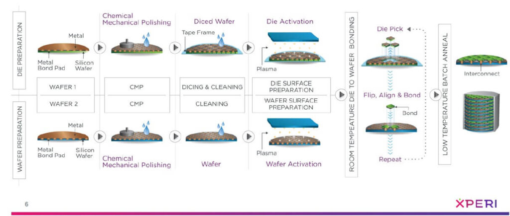
Xperi reports that extending DBI technology to D2W memory applications involves solving some additional challenges. For D2W applications, a larger pad size is desirable to accommodate the alignment accuracy standard in high-volume manufacturing (HVM) die bonders. Current technology for flip chip bonders can achieve alignment accuracy in the 1-10μm range. The lower accuracy machines can meet much higher throughput requirements than the high accuracy models. Wafer singulation is also a dirty process; therefore, maintaining a clean die surface for bonding is challenging.
Xperi has now demonstrated D2W hybrid bonding at a 10μm pitch with electrical test yield up to 92%. They have also demonstrated a process for cleaning and activating die on a dicing tape in a dicing frame. Pick-and-place will then take place directly from the dicing frame at a demonstrated throughput of 1636 die per hour with a single head bonder.
The key to the void-free bonding is a well-controlled clean chip and wafer surface prior to bonding. Xperi has developed processes to clean the chips sufficiently to routinely achieve >90% void-free bonding in a prototype environment. The key to high electrical test yield is the uniform Cu recess in the final CMP process. DBI D2W hybrid bonding requires an oxide surface roughness of less than 1nm. It also requires shallow and uniform Cu recess for low temperature anneal. For bonding pads of 10mm diameter, standard CMP processes used in the BEOL fabrication create Cu recesses too deep for low temperature anneal. Xperi developed a special CMP process to produce shallow and uniform Cu recess and transferred the process to the Fraunhofer Institute. The special CMP process scaled well to its 300mm CMP tool. With the special CMP technology, the team reports controlling the Cu recess variation across the entire wafer to be less than 3nm. For any given D2W pair, the sum of TTV on the wafer side and the chip side will be less than 6nm.
DBI Ultra process flow is shown in Figure 2:
So far there have been no announcements by Hynix, Samsung of Micron about adopting this technology but we should note that at this same ECTC where Samsung made a presentation on its studies of “Cu microstructure of High-Density Cu Hybrid Bonding Interconnections”. Logic tells us that all three have been or soon will be studying this technology enough to come to a conclusion on whether or not to use it. IFTLE will keep you updated on future status.
For all the latest on Advanced Packaging stay linked to IFTLE……………………….


