
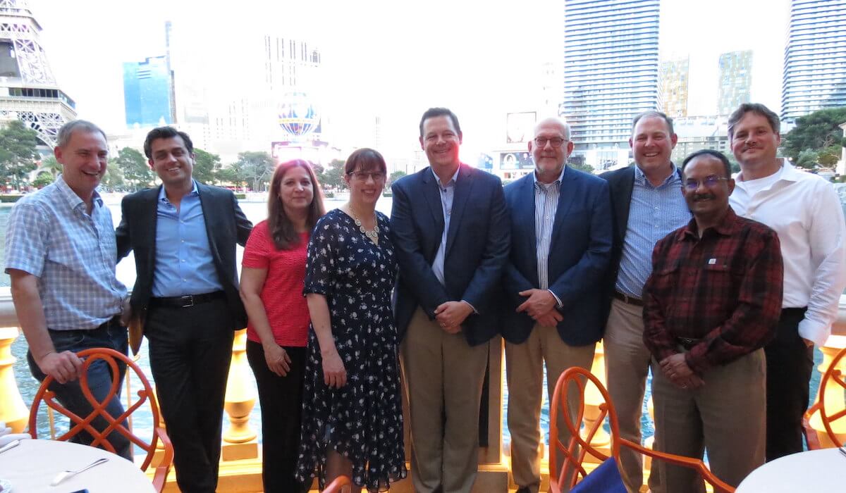
In the blink of an eye, the 69th Electronics Component Technology Conference (ECTC 2019) has come and gone in a swirl of presentations, conversations, and networking events. Last week, (May 27-31, 2019) Las Vegas played host to 1563 attendees (the second highest number ever), who gathered to share and learn about the latest trends, drivers and technologies that make the microelectronics industry tick.
Once again held at the risqué Cosmopolitan Hotel, amidst bright lights and scantily clad gamblers and partiers, it seems an odd setting for a technology conference. This year, the locale sparked an interesting question during the Women’s Panel on Diversity and Inclusion: Why this venue, where the carpeting in the room depicted a naked woman?
Why indeed? Innuendo notwithstanding – the answer was quite practical. The committee entered into a long-term agreement and locked in a rate before the building had even been constructed. And so, every three years for the past decade, we turn a blind eye to the debauchery going on around us and get down to the work at hand. In truth, with 358 papers and eight special sessions to choose from (many in the evening), not to mention 102 exhibitors to visit, there really isn’t time left to make any mischief.
Following are some of the highlights of ECTC 2019, from our perspective.
Future (Visions) of Electronic Packaging

This year’s ECTC panel session looked at the future of electronic packaging through the lens of researchers from TU Dresden, Georgia Institute of Technology and Greenwich University. Once again, Moore’s Law was declared dead, to be replaced by heterogeneous integration (HI) as the best path forward.
As Chris Bailey, Greenwich University, explained, not only do the economics of Moore’s Law no longer make sense because the cost of design has grown exponentially, HI does a better job than system-on-chip (SoC) of integrating different technologies and materials, such as high-performance chips, with bioMEMS, MEMS, RF devices, high bandwidth memory (HBM), and much more. “The heterogeneous integration roadmap (HIR) is not about silicon, like the ITRS,” he explained. “It’s about packaging.”
Reporting from this year’s HIR roadmap meeting prior to ECTC, he focused on chapter updates for co-design modeling and simulation, as reported by key stakeholders from industry, system designers, universities and took vendors. “Architectures are changing, and the tools needed for exploration are changing,” he said, noting Mentor, A Siemens Business specifically for its work in HI design and a simulation environment.
Neuromorphic Computing Needs 3D
The team from Georgia Tech talked about new packaging architectures for neuromorphic computing, in which computers behave like a human brain. Neuromorphic chips address senses and pattern recognition, whereas traditional chips focus on language and analytical thinking.
Again, SoC designs are not suitable for neuromorphic computing. 3D stacking is preferable, but through silicon vias (TSVs) still pose a challenge. The recommended approach was a combination of 2.5D and 3D architectures, integrating dielets (or chiplets) on an active interposer. Modularity is the key; dielets allow for design reuse. They called it the 5D Brain in Package (5D BiP). I’m not sure that what the industry needs right now is another acronym, but let’s see if it sticks.
By the way, chiplets are also on NXP’s radar as a HI solution for autonomous vehicle applications, noted Tu Ahn Tran during the panel on materials considerations for autonomous driving.
Biocompatible Packaging
Looking as far ahead as 2025, Martin Schubert, TU Dresden, said biocompatible packaging is a key enabling technology for the future, particularly in the medical electronics space. Materials considerations are critical for stretchable and flexible systems for everything from implants to diagnostic tools for telemedicine.
In his keynote speech, John Rogers of Northwestern University expanded on this topic with a discussion on what can be achieved by integrating soft electronics into the body. The skin in the body’s largest organ with a reversible interface, he explained. The idea is to design similar packaging for implants. He described three directions to take in materials science and mechanics research:

- Soft, biocompatible
- Biodegradable
- 3D bio-interfaces
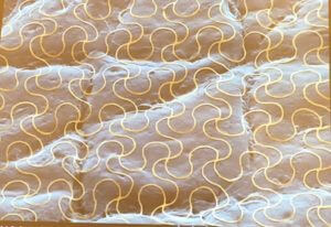
By leveraging the best of what’s available in well-established electronics materials and processes, and Rogers’ figure out how to convert that into a biocompatible form. For example, Rogers’ team has successfully created thin, flexible, wavy and stretchable nanoribbons from device-grade Silicon, and have combined them with soft elastomers to create a skin-like device platform for monitoring vital signs in preemies. (figure 1)
The intention is to replace the rat’s nest of wires that tether infants to their beds and inhibit interaction with their parents, with wireless sensor modalities that drop into the skin framework. The patches are designed with premature infants’ fragile skin in mind, which is 40-60% thinner than adult skin and is 45% more susceptible to scarring.
An interdisciplinary team comprising researchers from Northwestern and neonatal experts from Prentice Women’s Hospital and Ann & Robert H. Lurie Children’s Hospital of Chicago, recently completed studies involving 100 premature infants down to 26 weeks gestational age, and successfully demonstrated that the data was as precise and accurate from the wireless sensors as the traditional wired versions. Since a picture is worth a thousand words, and a video, even more, watch below for the details.
Thanks to funding from the Gates Foundation and Save the Children, 20,000 of these systems have been deployed in India, Pakistan, and Zambia, where wired devices aren’t available.
Other applications suite to these wireless skin sensors included stroke rehabilitation, that allows for tracking patients’ performance at home.
Epidermal microfluidic devices have also been developed with this technology, to be used for sweat analytics. For example, analyzing sweat chloride for Cystic Fibrosis screening, or in consumer health applications for measuring hydration levels during fitness workouts.
More to come…
These are just a few stories we’re bringing you from ECTC 2019. Stay tuned for more coverage on 3D InCites over the next few weeks, as we bring you some exclusive interviews from the technology corner, an update on autonomous driving, and more complete coverage of the Women’s Panel on Diversity and Inclusion. ~ FvT


