
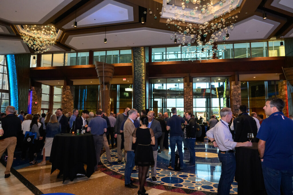
At last week’s International Microelectronics and Packaging Society’s Device Packaging Conference, (IMAPS DPC 2024) we didn’t need TrendForce to tell us that advanced packaging is the hottest technology in the semiconductor industry. We just needed to look at the record attendance of more than 700 advanced packaging enthusiasts who turned up to learn about the latest trends driving automotive reliability, AI, and chiplet architectures. They also got the latest updates on CHIPS Act funding for advanced packaging and R&D. Speakers presented to overflowing conference rooms. Hotel staff had to add extra buffet lines to keep things moving at lunchtime. It was exciting to see so many new, younger faces in the crowd. That bodes well for the future of IMAPS and the microelectronics industry.
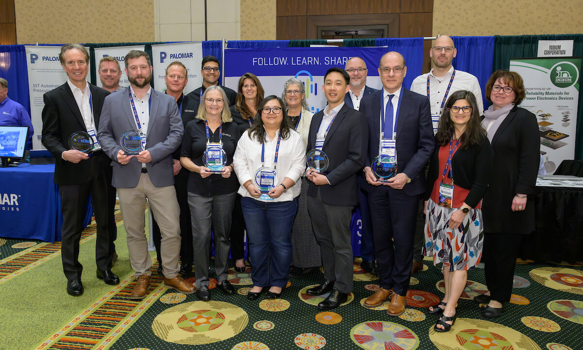
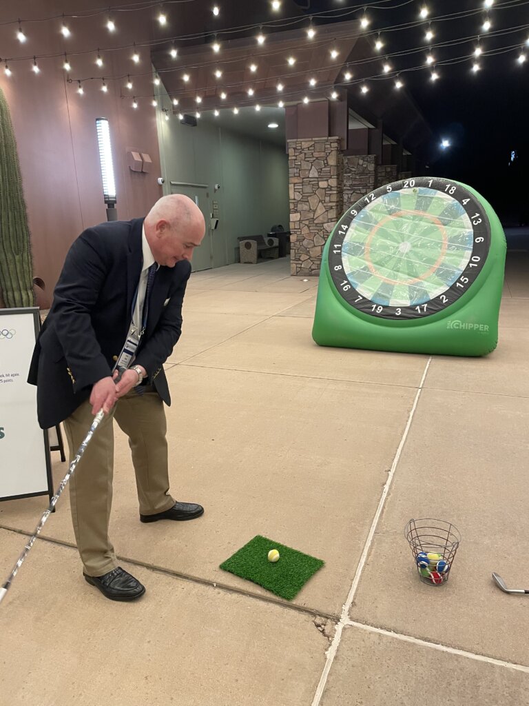
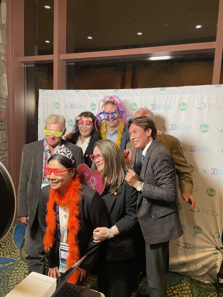
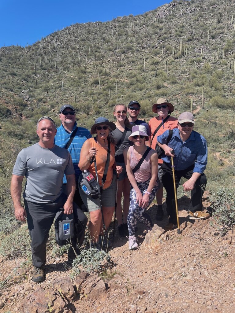
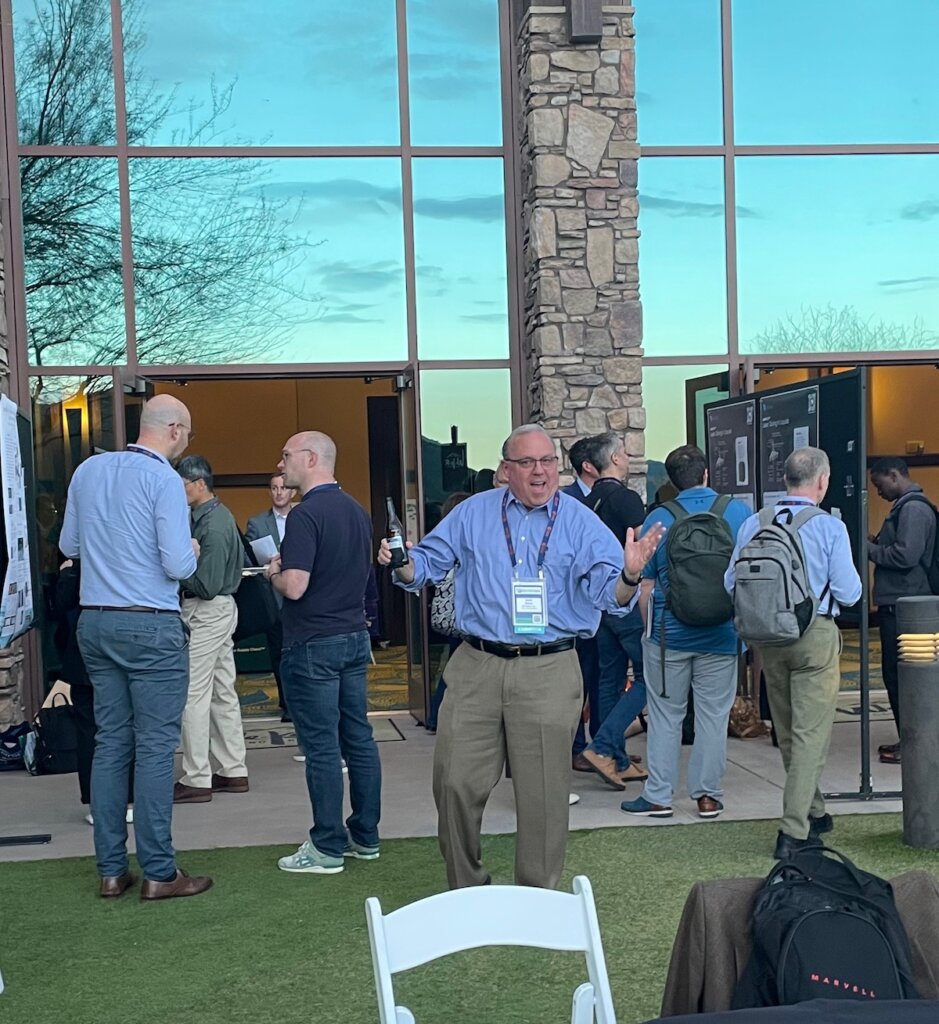
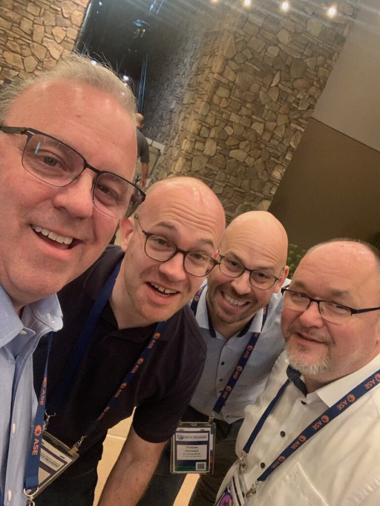
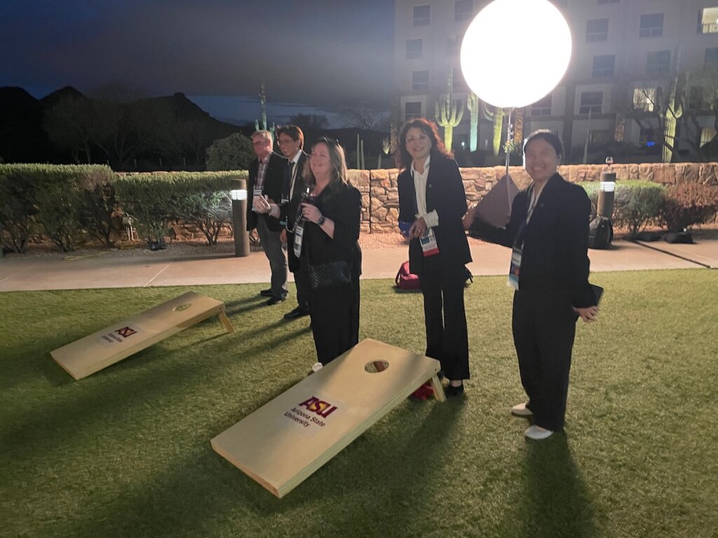
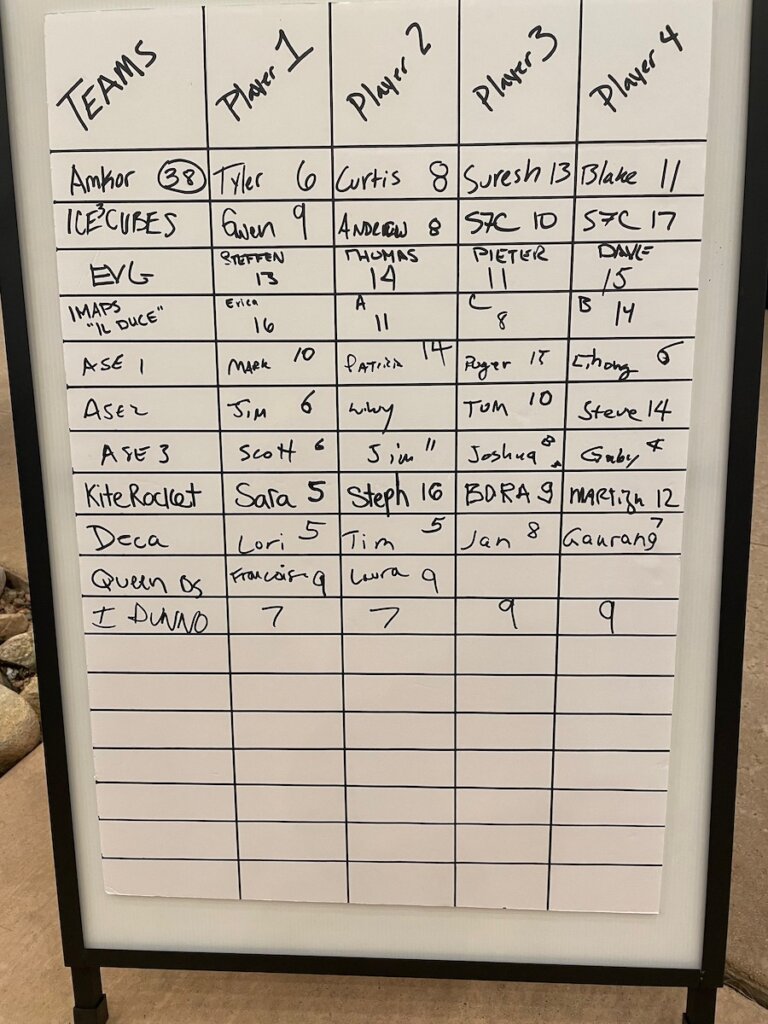
This was the 20th Anniversary of IMAPS DPC, and everyone was in the mood to celebrate. As official industry partners, we hosted our 11th Annual 3D InCites Awards ceremony. We also augmented Wednesday’s poster session evening entertainment with the first-ever 3D InCites Back Yard Olympics, with a photo booth sponsored by DECA, games sponsored by ASU (cornhole) and our community members Amkor Technology (beer pong) Namics (golf chipping), ERS Electronic GmbH (axe throwing); IMAPS (hula hoop); and ring toss. For the third year in a row, KLA sponsored our Thursday Hike for DEI, which supports the 3D InCites DEI Fund, which provides scholarships to women and under-represented minorities pursuing careers in STEM at the technical school, community college, and university levels. Everyone who made time in their busy schedules for these social activities will tell you – we’re making advanced packaging fun again!
IMAPS DPC Keynotes: Focus on Application Trends and Chiplets
The IMAPS DPC planning committee, led by General Chair Scott Hayes (NXP Semiconductor and General Chair-elect Amy Lujan (Savansys Solutions) pulled out all the stops this year, adding a fifth keynote, and several new technical sessions, that tallied up to more than 100 speakers. As the official podcaster of IMAPS DPC, I focused on the keynotes and the Wednesday evening panel discussion. Here’s a recap of what we learned.
What’s Under the Hood?
Pradeep Lall, of Auburn University, reviewed the five levels of automation that he says will drive ADAS systems through 2027 and shared a long list of safety systems in which “failure is not an option.” Electronics in harsh environments must now prove they can operate for 10 years and up to 100K miles.
Lall did a deep dive into the impact of various materials and interface challenges that can affect overall reliability. As the electronic content of today and future cars continues to increase, this is becoming a greater challenge than it was previously.
He also touched on the crucial topic of PFAS (aka “forever”) chemicals that are coming under regulation worldwide. Comparing it to the RoHS initiative of the early 2000s, he talked about the complexities of replacing materials with proven reliability with environmentally friendly alternatives.
“While the evolution of tin-lead properties was very muted, nobody was concerned,” he said. However, as electronics play an increasingly important role in automotive safety applications; the material properties and interfaces are important. “We’ve got our work cut out for us,” he said. Methods must be improved. The bottom line is to model and test everything.
Heterogeneous Integration, Chiplets, and AI
Three of the five keynotes plus the panel discussion gave us a comprehensive picture of chiplet architectures, how they are enabled by heterogeneous integration (HI), and how the AI explosion drives them.
From IBM’s Arvind Kumar, we learned about foundation models for AI that are trained on large amounts of unlabeled data. Once trained, these data can be adapted to use cases to solve business problems previously considered intractable, explained Kumar.
He said this general capability is a game changer accelerating AI’s progress. However, existing hardware isn’t meeting the demanding compute requirements to train these models. It’s not just about compute, it’s also about memory.
Traditional approaches to scaling are no match for today’s AI-driven workloads. At IBM Research Lab, work is being done to disaggregate SoCs to decouple AI from the other system parts. These AI chiplets can be highly targeted. Heterogeneous integration processes make it possible to combine AI with the stacked memory that it needs to support applications from mmWave to edge computing.
From Hemanth Dhavaleswarapu of AMD, we learned that there is no one-size-fits-all approach to supporting the demanding needs of AI. This is why AMD has developed a deep bench of advanced packaging technologies, many of which use chiplets. He provided an overview of all AMD’s activities to meet the challenges of chiplet integration.
Dhavaleswarapu showcased AMDs latest and greatest of these – the AMD Instinct – M1300, the industry’s first APU product, which integrates chiplets using a “Lego®” approach. He described it as a “3.5D” package comprising a dense through silicon via (TSV) interface, 3D hybrid bonding, and a 2.5D silicon interposer. He also shared a general 3D interconnect Roadmap not specific to AMD that extends to 2030. Die-to-wafer and wafer-to-wafer hybrid bonding are featured throughout the roadmap.
Intel’s Pooya Tadayon pulled the chiplet conversation together by talking about the problems with chiplets, to get us thinking about what we need to do. While the industry is trending towards 3D integration and advanced packaging schemes to address cost and scalability challenges, he says the ecosystem is still not ready. Fundamental design, manufacturing, and enablement challenges must be addressed. He also noted that metrology, physical debug, and manufacturing tests are underserved areas that need more focus and investment from industry partners and academia.
Tadayon listed several trends and the challenges they bring that need solutions before they can be realized. For example, Super Stacks are chiplets stacked 30 high that is being proposed as a path to achieving best-in-class size and weight. But they need new tools and new workflows to be possible. Tadayon also described a fully 3D Cube design that is truly 3D because the functionality is on all sides of the device. But this needs new manufacturing tools and processes, as well as new design tools and methodology to make it happen. He also talked about the promise of glass substrates.
The Wednesday night keynote from Raj Pendse, of Meta Reality Labs completely freaked me out with the augmented reality Codec avatar of Mark Zuckerberg, which he described as “the next logical step in the wearable computing trajectory.”
Pendse’s message was that AR processing loves 3D but needs a different kind of 3D than is used for high-performance computing. Extreme miniaturization and ultra-low power consumption are driving factors for AR. Pendse described functional 3D subsystems – or “Clusters” woven together using flexible substrates. The module packaging combines TSVs, flip chip, and fan-out wafer-level (FOWLP) packaging. He called for standardization similar to UCIe for these specialized devices, as UCIe is designed for HPC and 2.5D configurations.
While Pendse was on the panel discussing the next “Killer App” for chiplets, I don’t think this will be it. AI at the edge seems to be more likely the big winner.

For a deeper dive into the chiplet discussion, be sure to listen to the Keynote Podcast, featuring Arvind Kumar, of our member company, IBM; as well as Hemanth Dhavaleswarapu of AMD, and Pooya Tadeyon, Intel. The episode drops on March 28th at 6 am. You can find it here, or wherever you get your podcasts.
Update on the Chips for America Act
As is tradition, the IMAPS Global Council’s Spring Meeting took place on Wednesday of IMAPS DPC. This year’s organizing committee did a splendid job of bringing in representation from the government, academia, industry, and local economic councils to share some success stories of Chips Act implementation.
Dan Berger, an IBM veteran who came out of retirement to work at the US CHIPS Office, updated us on the National Advanced Packaging Manufacturing Program (NAPMP), and R&D. He talked about the recent Proposers Day – in which 500 potential proposers from US-based advanced packaging substrate and substrate materials manufacturers participated for funding opportunities. This is significant as historically most advanced packaging substrate suppliers are outside the US.
Berger also noted progress in establishing advanced packaging roadmaps that will be used to develop technology investment areas, as the US focuses on leadership in packaging within the next 5-10 years. To this end, the NAPMP will create a National Advanced Packaging Pilot Facility to provide a test bed for new technologies to be prototyped and tested.
Berger encourages attendees to identify individual contributions to the ecosystem and build teams to collaborate on these initiatives.
Arizona’s Silicon Oasis
From Vic Narisus, of the Arizona Commerce Authority, we learned about the exciting things happening in Arizona to make it the “Silicon Desert”. I prefer the term, Silicon Oasis – as desert implies barrenness, and Arizona is anything but lacking in opportunities designed to draw in the entire semiconductor ecosystem.
President Biden couldn’t have timed his visit to Intel any better. As he arrived to celebrate up to $8.5 B in funding, Narisus told us about the ACA’s involvement in helping 34 semiconductors land in Arizona since mid 2020s. He outlined the available tax incentives and exemptions for companies who want to locate facilities in Arizona. He also talked about all the semiconductor education and training happening.
This was a great segue into a talk by Zachary Holman, who talked about what’s happening at Arizona State University, and the role academia plays in creating the semiconductor workforce of tomorrow. He was excited to share that ASU’s Fulton School of Engineering has nearly 32K engineering students enrolled. But that will not be enough to meet the needs of TSMC, Intel, and other companies.
Holman outlined ASU’s strategy to transform into a packaging leader by hiring top faculty, revamping the curriculum, and training students on leading-edge equipment. The big news of the week was ASU’s collaboration with our community member, Deca, to establish the first-of-its-kind 300 mm fan-out wafer-level packaging pilot line in ASU’s MacroTechnology Works fab. Customers and students can run Deca’s processes or their own on leading-edge equipment. (Once mature technology is transferred to a commercial manufacturing line, using Deca processes will require a license.)
Addressing the Talent Shortage
Skywater’s Mark Litecky talked about dynamics redefining our industry, and how the U.S. share has shrunk from 37% to 12%. The share of global packaging is at a sobering 3%.
While the numbers I’ve heard lately about how many engineers and technicians are needed to meet the semiconductor industry demand range from 60K to 100K, Litecky broadened the scope to include not just engineering, but all areas of discipline. He said we need a talent pool of 250K in the next five years.
To help increase US advanced packaging capacity as well as address the talent crisis, Skywater has identified several goals. The company is working to revitalize domestic manufacturing through participation in the DoD’s IBAS RESHAPE program. It is helping develop the workforce through scholarships and apprentice programs. And by strengthening partnerships with companies like Deca and Adeia, it aims to accelerate technologies of the future.
While it’s great to see the US coming together to reclaim semiconductor manufacturing superiority, again, I caution all to remember that this is a global industry. With that in mind, I was glad to hear ASE’s Mark Gerber close the GBC with these words of wisdom: “We can’t do everything in the US. We still have to collaborate and partner with the entire world.”
An upcoming podcast episode featuring interviews with Dan Berger, Zac Holman, and Mark Litecky explores these topics more fully.

