

I cannot say I enjoyed this year’s COVID 19 version of ECTC 2020, but I guess it was better than nothing. I will leave the discussion of what I would like to see improved in the software package for the organizers.
Let’s first take a look at three key papers presented by TSMC whose goal, it is obvious, is to become the King of Advanced Packaging.
InFO-SoW Packaging for High-Performance Computing
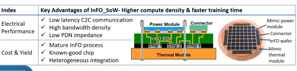
In this paper, TSMC attempts wafer-scale integration with its integrated fan-out (InFO) system-on-wafer (SoW) packaging technology. In many ways, InFO-SoW is reminiscent of the early 1980s attempts by Trilogy to create a full SoW. This modern solution attempts to eliminate the substrate and the printed circuit board (PCB) by serving as the carrier itself. They note that their main driver for such a system is high-performance computing (HPC) as we enter the exascale computing area. The perceived advantages of InFO-SoW are shown below (Figure 1).
In Figure 2, TSMC compares InFO-SoW to what they call a “regular flip-chip multichip module (MCM).”
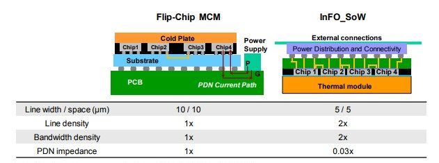
For flip-chip MCM, the signal has to pass through PCB and then back. Not so for InFO -SoW. In addition, to get an RDL length of 20mm, the InFO solution shows a 0.4 dB lower loss at 28 GHz resulting in a 10% power savings. The lower loss is due to the lower roughness of the substrate. BUT …In comparison to traditional motherboard configuration, the INFO SoW must distribute more heat per unit volume and therefore must use a liquid cooling solution. InFO-SoW reliability testing is shown in Figure 3.
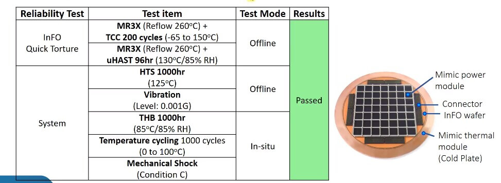
Chip-package interconnect (CPI) risk assessment was done using finite element analysis (FEA) to compare the stress in the extreme low-K (ELK) dielectric layers compared to successfully qualified-flip chip architecture equivalents. ELK stress of InFO-SoW is 60% lower than that of the flip-chip structure due, they presume, to the thick compliant dielectric layers of the InFO.
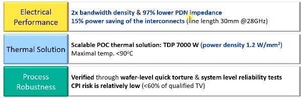
In conclusion:
Ultra High-Density SoIC (SoIC-UHD) with sub-micron Bond Pitch
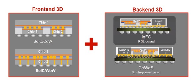
SoIC was first introduced by TSMC at last year’s ECTC Conference. With the goal of continuing Moore’s Law, TSMC explains its advanced packaging used for both back-end and front-end 3D. Back-end 3D refers to existing fan out and interposer packaging technologies. Front-end 3D refers to chip-to-chip stacking whether it is chip-on-wafer or wafer-on-wafer. The reason they call SoIC front-end 3D is that it is based on wafer processing. This makes it possible for their chip-to-chip interconnect density to go down to < 1µm pitch (Figure 5)
Things that affect the bonding yield include cleanliness, optimized Cu topography (from CMP), and Cu barrier optimization. Optimizing each resulted in ~ 30% yield improvements.
Bonding pair resistance and breakdown voltage are extremely sensitive to overlay. Only when the overlay is less than 0.1µm will resistance be minimal and stable.
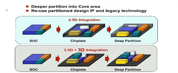
So, what could this bonding be used for? They contend that this will enable chiplet partitioning and subsequent reintegration. Ultra-fine pitch bonding allows a deeper partition and reintegration (Figure 5).
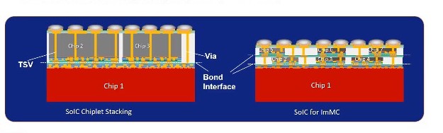
SoIC can also be used for multilayer stacking. Specifically, TSMC detailed its technology called Immersion-in-memory compute (ImMC) which “interlays logic and memory by stacking.” One would optimize logic and memory separately, get known good die (KGD), and then stack as shown in Figure 8.
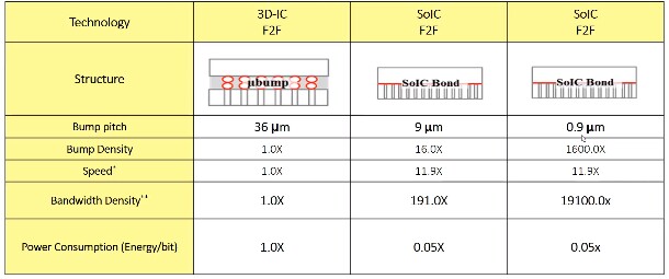
The chart below compares the traditional 3D IC using solder bumps vs SoIC using 9µm and 0.9µm pitch densities.

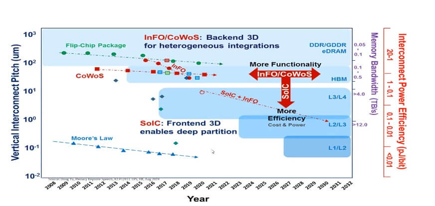
The density and power efficiency of the TSMC branded technologies are shown below.
SoIC for Low Temp, Multilayer 3D Memory Integration
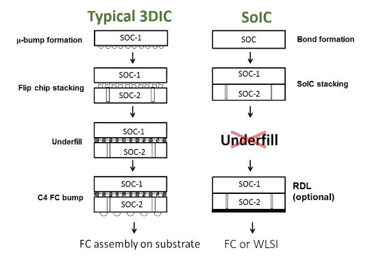
This paper focused on multi-layer memory stacking, comparing the integration flow between typical 3DIC package and SoIC package. Since SoIC is a bumpless structure, it can achieve a much tighter pitch and it does not require any underfill processing (Figure .
Bump density, electrical, and power/thermals are compared below:
LT-SoIC 3D memory reportedly outperforms typical 3D memory stacks due to the smaller form factor, higher bandwidth, and lower power consumption.
It becomes obvious that this TSMC technology will be in competition with Xperi DBI technology for memory stacking in the coming years. IFTLE will be keeping an eye on this competition.
TSMC Builds $10B Packaging Facility in Hsinchu
Focus Taiwan has reported that TSMC will open a new high-end integrated circuit packaging and testing plant ($10.11 B). The plant will be built in the Chunan section of Hsinchu Science Park. It is scheduled to be completed in May 2021, and operations will start in mid-2021. TSMC already operates advanced IC packaging and testing plants in Taoyuan, Hsinchu, Taichung, and Tainan.
For all the latest in Advanced Packaging stay linked to IFTLE……………………….


Comments are closed.