

Just like most other events that attract a large number of people, TSMC 2020 events were held online too. While I missed the many friends I normally meet at TSMC events, I was able to follow the powerful messages from TSMC, its Open Innovation Platform (OIP) partners, and satisfied customers from the comfort of my home. Best of all, because the recordings will be available for some more time, I can replay the presentations as needed, to dig deeper. Talk to your TSMC contact how/where you can access them too.
Dave Keller’s TSMC 2020 Introduction
On August 25, Dave Keller, President, and CEO, TSMC North America, introduced the TSMC 2020 Technology Symposium and the OIP Forum. He welcomed the 2000+ virtual attendees from 300+ companies, then thanked all customers and ecosystem partners for their contributions to TSMC’s success. He highlighted several important market trends, major TSMC achievements, and the importance of semiconductor technology for connecting people during the coronavirus pandemic. Then Keller introduced his boss, C.C. Wei, TSMC’s CEO.
C.C. Wei’s TSMC 2020 Keynote
Wei emphasized that TSMC wants to be the trusted technology and capacity provider of leading-edge technologies for companies that serve opportunities like 5G, VR/AR, Smart Mobility, and AI/ML. He outlined N7 and N6, N5 and N4 and N3, which will be available for risk production in 2021 and volume production in the second half of 2022.
Wei introduced Renee James, who founded Ampere Computing in late 2017 and is now Chairman and CEO. She praised TSMC as an excellent partner for developing the ARM-based 7 nm AmpereTM AltraTM processor, introduced in Spring 2020, and announced that Ampere’s 5 nm test chip is now in TSMC’s Fab 18.
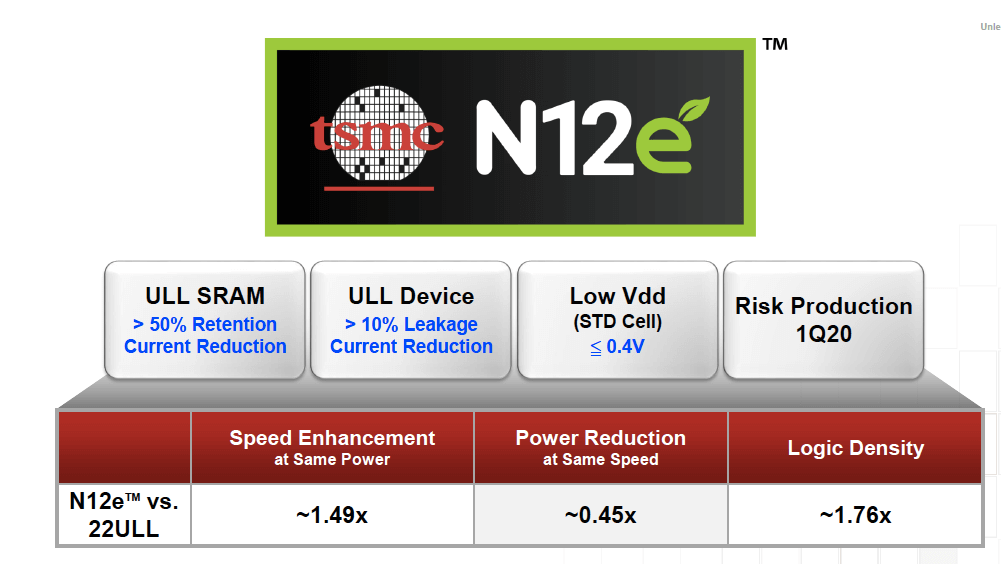
Wei highlighted the benefits of TSMC’s new, ultra-low-power process N12eTM, see Figure 1. He explained the importance of this process, targeted at battery-power devices, such as smart IoT edge nodes and handheld medical equipment.
At this point, Wei introduced another TSMC partner, Dr. Jonathan M Rothberg, Founder & Chairman of Butterfly Networks. They utilize both TSMC’s low power and specialty technologies (Figure 2). Rothberg’s team has developed and introduced Butterfly IQ, a handheld AI-based ultrasound scanner with 10,000 transducers on a single chip from TSMC. The IQ is priced at only $ 2,000, to make ultrasound scanning ubiquitous. Together with a smartphone or tablet, this scanner replaces/complements a physician’s stethoscope, especially in less fortunate countries, where large $ 100,000+ ultrasound scanners are not available.
Last, but not least, Wei pointed out that 2D scaling cannot serve every opportunity anymore. As 3D scaling is gaining importance, TSMC has developed chip-stacking and advanced packaging technologies, combined in the TSMC 3D FabricTM portfolio, see Figure 3.
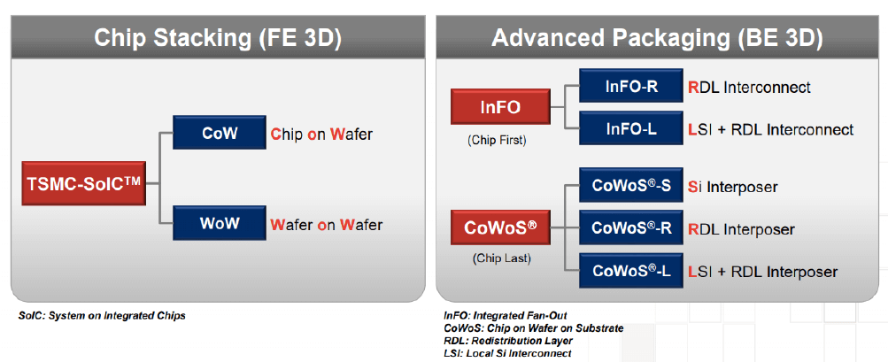
including both FE 3D and BE 3D technologies. (Courtesy of TSMC).
After this keynote, the leaders of three TSMC divisions, Senior Vice Presidents Y.J. Mii, Kevin Zhang, and Y.P. Chin expanded on their team’s leadership in Advanced and Specialty Technologies and Manufacturing Excellence, respectively. Dr. Doug Yu presented the many innovations by his Advanced Packaging division. Knowing that Phil Garrou will cover shortly TSMC’s Advanced Packaging capabilities for 3D InCites in-depth, I’ll focus below on day two of this TSMC event: the OIP Forum.
The TSMC 2020 OIP Forum
Day 2 started with Dr. Cliff Hou, Senior VP of R&D, giving a keynote about the TSMC Ecosystem for Innovation. He showed the availability of IP building blocks for different technologies, as well as which EDA tools are qualified for which design steps, from architecture evaluation to verification of the final tape out – for N7 to N3, specialty technologies, and advanced packaging. Then the CEOs of Cadence, Lip-Bu Tan, and Synopsys, Aart de Geus, as well as Joseph Sawicki, executive VP of Mentor, a Siemens Business, demonstrated their commitment to supporting TSMC and the mutual customers with design tools and building blocks for developing single and multi-die ICs.
In addition to this series of keynotes, TSMC offered recordings of thirty-six presentations, selected from many more papers that the 60 participating OIP partners submitted. They were grouped by application areas: HPC & 3DIC, Mobile & Automotive, and IoT & RF.
Allow me to recommend a few of them, likely to be useful for 3D InCites readers:

In the HPC & 3DIC segment:
- James Huang from Alchip presents best practices for designing a Machine Learning (ML) ASIC, comprising four chiplets
- Igor Elkanovich from GUC presents how to use its low-power interface IP to interconnect chiplets
- Stephen Crosher from Moortec’s explains how to use its PVT monitoring IP in a hyper-scale design
- Norman Chang from Ansys showed how to use its thermal analysis solutions from 3DIC architecture to tape out
- Manuel Mota from Synopsys outlined its portfolio of die-to-die physical IP for N7 and N5 chiplets
In the IoT and RF segment:
- Karthik Srinivasan from Ansys presented how to analyze EM and self-heating in mm-wave RF devices
- Bart Keppens from Sofics presents how to meet ESD/EOS/Latch-up requirements in IoT devices
- Rita Horner from Synopsys discusses multi-die integration challenges and which Synopsys tools to use
For your information, Cadence announced during this event two important capabilities for 3DICs:
- A TSMC certified reference design flow for their latest packaging technologies:
- Availability of silicon-proven die-to-die “UltraLink D2D” PHY IP for chiplets manufactured in TSMC N7, N6, and N5
Personal comments:
TSMC clearly has made enormous progress since 1998/’99, when my team at Synopsys had the opportunity to work with Dr. Cliff Hou’s small team on the first reference flows for up to one Million gates using Design Compiler and PrimeTime. In the 20+ years since then, Hou’s team has grown beyond one thousand engineering experts. TSMC has managed to shrink feature sizes by more than 100x and, with the addition of advanced packaging, the practical gate-count for a multi-die IC is approaching one hundred Billion gates.
The visionary and high-integrity leadership, initially from Dr. Morris Chang, now by C.C. Wei, supportive investors, and excellent engineering teams to manage win-win partnerships and serve loyal customers are key elements for this success.
In many previous blogs, I pointed out that a significant part of the IC value creation is moving from the (silicon) die to the IC package. TSMC’s 2020 event has clearly amplified this message and conveyed how many benefits – e.g. lower die cost, shorter development time, lower power, higher reliability, higher performance, smaller and lower-cost systems, etc. – advanced packaging technologies offer System and IC designers. It also showed that advanced IC packaging is becoming a high-precision effort, demanding significant investments in R&D, materials, and equipment from manufacturers as well as from EDA and IP partners – demanding in exchange higher margins for package assembly and test experts.
I am happy to see that key executives from large EDA vendors expressed their commitment to supporting TSMC’s silicon and packaging capabilities. Only by automating large portions of the increasingly complex design flows, TSMC’s capabilities will become accessible to many more companies. The increasing returns will finance many more innovations. ~ Herb


