If you are designing a heterogeneously integrated, multi-die, high-performance device for markets such as HPC, AI, data centers, etc., then the silicon interposer is probably the platform of choice. Yes, it comes at a cost, and generally requires expensive silicon place-and-route (P&R) tools, along with workflows for implementation. With the emergence of new organic and glass substrates, and advanced IC packaging design solutions, this is all starting to change.
There has always been a drive to find more cost-effective solutions for silicon interposers that can still deliver the required performance. Intel pioneered this path with its embedded multi-die interconnect bridge (EMIB), which allowed the use of low-cost, proven, organic materials for the overall substrate. Soon most OSATs and substrate suppliers had their own version of EMIB. While cheaper overall, it still involves a complex substrate assembly process.
Several companies, such as Absolics, have been exploring glass as a high-performance, yet low-cost platform. This technology is showing great promise and is expected to see increased adoption as we go into 2023 and beyond. Glass substrate-based designs offer low loss and very high data transfer speeds while offering lower power consumption and thermal stability. The design methodology workflow for glass is very similar to advanced organic interposers such as RDL build-up, made popular with TSMC’s 3DFabric’s Integrated Fanout (InFO) technology as well as similar solutions such as ASE’s FOCoS and Amkor’s SWIFT.
With glass interposers ideally suited for HPC, AI, etc., the subsequent designs are considerably challenging and require the design tools and workflow to support multiple capabilities not typically required for conventional laminate core packaging (Figure 1).
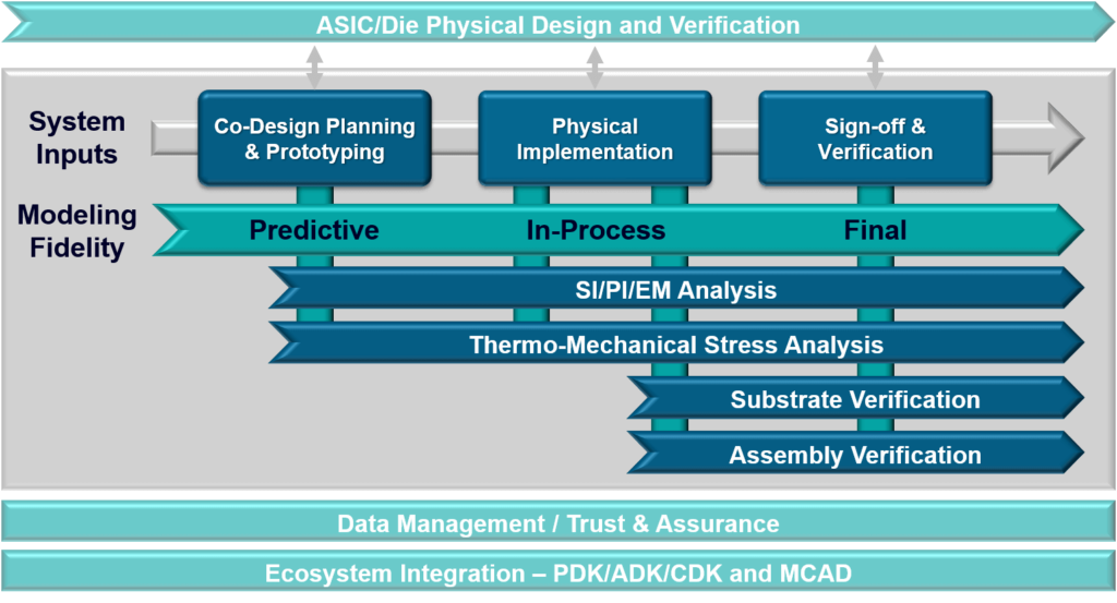
This is where advanced semiconductor packaging design solutions triumph as they deliver all the capacity, performance, and capabilities needed without traditional expensive and Linux-limited P&R limitations, given that most semiconductor heterogeneous integration is the responsibility of packaging design teams.
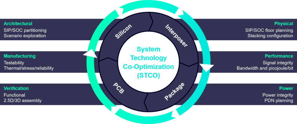
The first area designers of advanced organic and glass substrate-based designs need to focus on is planning and prototyping; not just of the base substrate but the entire package assembly. Planning and prototyping the entire package assembly holistically using system-technology co-optimization (STCO) techniques results in a completely optimized digital twin model of the design (Figure 2).
During design planning, the designer must use predictive analysis to ensure that the chosen design scenario can achieve routing, signal, power, and thermal requirements. Predictive analysis is not a detailed analysis. At the planning stage the design is just a prototype, lacking the 100% fidelity of a completed design, so predictive analysis is not sign-off accurate. Instead, it’s fast allowing for rapid tradeoff decision-making that helps the package design architect refine the prototype and arrive at the ideal implementation scenario. Now given the typical application focus of advanced organic and glass interposers the resulting designs are going to be very large with extremely high pin counts and expansive connectivity structures. Therefore, the capacity and interactive performance of your implementation design tools should be one of the first things you consider.

The next area is high bandwidth memory (HBM) channel design support. Ideally, the design methodology should have a high degree of automation to ensure productivity and reduce potential errors so often introduced when using manual design methods or tools without sufficient rule support and HBM channel replication. Because such designs are large, complex, and dense, the need to design concurrently with multiple designers working in parallel is commonly seen as a prerequisite for success. Leveraging multiple designers with different areas of expertise is further enhanced if the concurrent design can be achieved across geographic borders.
The next area of focus is around multiple fabrication and manufacturing requirements such as advanced metal layer balancing and degassing. This is another challenge that must be addressed in tandem with the creation of complex power and ground structures that need to provide sufficient power delivery without unacceptable levels of IR drop. These designs can often benefit from reusing known good design IP within and across designs to speed implementation and reduce risk.
These advanced designs benefit from design tools and design workflow automation and customization, such as the ability to easily develop custom substrate-specific design rule checks (DRC) that can be used during design. Of course, even when the design is complete it needs to undergo rigorous substrate and assembly connectivity (LVS) verification using the actual manufacturing data, typically GDSII or OASIS, why? Because you need to verify the actual data that will drive fabrication and assembly/test. Performing detailed DRC during design is important but it’s not signoff. Using the actual manufacturing data is signoff.
In summary, it’s clear that 2023 will see further advances in our quest to get more from Moore with new organic and glass substrate technologies and platforms, as well as advanced semiconductor packaging EDA design solutions.
This article originally appeared in the 2023 3D InCites Yearbook. Read the full issue here.