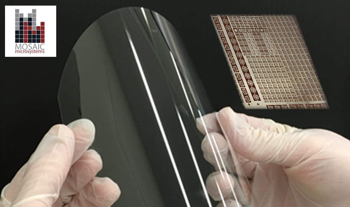
Glass is a compelling substrate for interposer and advanced packaging applications. Compared to organic printed circuit boards, glass has excellent dimensional stability and very smooth surfaces that allow fine line/space metallization. Compared to silicon, glass can be produced thin (< 200 mm) at large volumes, providing a path to large-area at low cost. Glass also has a very low loss tangent, making it an ideal platform for ever-increasing frequency bands.
Two current limitations exist to thin glass adoption. First is the difficulty of introducing flexible, transparent substrates into an existing fabrication infrastructure. Secondly is the need for copper-filled, hermetic through-glass vias (TGV) in today’s applications—and for filling the vias in a process that itself does not need a new infrastructure.
In this paper, we review the formation of vias in glass and describe a simple and void-free approach to thin glass handling and metallization of vias that addresses both of the limitations to glass adoption. The approach also builds on the already well-developed copper electroplating technology for TSVs. By attaching a thin glass “device” wafer to a handle such as silicon using the Viaffirm® temporary bond, an effectively blind via is formed where the foot of the via meets the handle. As in silicon, the blind vias can be filled with physical vapor deposition adhesion and seed layers, and bottom-up copper electroplating- fill chemistries. However, the Viaffirm approach has a great advantage: after filling, the substrate can be debonded to yield a finished and filled TGV substrate, ready for subsequent processing without back-grinding or even cleaning. Details of this process including process flow and capability are discussed.