
Intel recently announced that it would use glass core substrates for advanced packaging in the second half of this decade. The company reports it has been researching and evaluating the reliability of glass core substrates as a replacement for organic substrates for more than a decade.
Intel says that it has a fully integrated glass R&D line in its Chandler, Arizona, campus, where it develops packaging technologies. The line reportedly cost over $1 billion.
Intel says it will introduce glass substrates initially “where it can be leveraged the most: applications and workloads requiring larger form factor packages (i.e., data centers, AI, graphics) and higher speed capabilities.” The company expects superior mechanical, physical, and optical properties from the glass substrates, which will “…enable the company to build higher-performance multi-chiplet system-in-packages (SiPs), aimed primarily at data centers”.
Glass substrates can tolerate higher temperatures (vs PCB substrates), reportedly offer 50% less pattern distortion, have better flatness for improved depth of focus for lithography, and have the dimensional stability needed for extremely tight layer-to-layer interconnect overlay.
As a result, Intel expects that a 10x increase in interconnect density is possible on glass substrates. Further, they expect the improved mechanical properties of glass to enable ultra-large form-factor packages with excellent assembly yields. In particular, Intel expects glass substrates to enable ultra-large 24×24 cm systems-in-package (SiPs) housing multiple pieces of silicon.
Glass substrates’ tolerance to higher temperatures also offers chip architects flexibility for setting the design rules for power delivery and signal routing because it gives them the ability to seamlessly integrate optical interconnects, as well as embed inductors and capacitors into the glass at higher temperature processing. This allows for better power delivery solutions while achieving the high-speed signaling that is needed at much lower power. Substrates, made from glass, have smoother surfaces than PCB-based ones and can also be made more than a quarter thinner than previous designs, assisting in reducing the mounting area. Power consumption can also be halved compared to traditional PCB solutions.
Intel expects these benefits to bring it closer to being able to scale 1 trillion transistors on a package by 2030.
Intel claims that glass substrates allow for a much higher interconnect density (i.e., tighter pitches), which is crucial for power delivery and signal routing of next-generation SiPs. It is talking about <5/5µm L/S and <100µm through-glass via (TGV) pitch, which enables a die-to-die bump pitch of <36µm on substrate and a core bump pitch of <80µm.
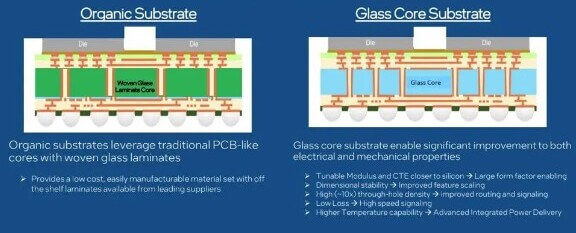
An Intel comparison of organic substrates vs glass core substrates is shown in Figure 1:
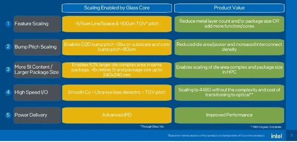
Figure 1: Motivation for glass core substrates (Source: Intel)
Intel compares the benefits of a glass core substrate below:
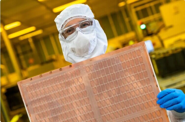
Intel expects to be producing these glass-based substrates on large panels such as the one shown in the above photo.
IFTLE should make it clear that Intel is not the first to announce in this technology area. In IFTLE 512 we disclosed that SKC ( a subsidiary of South Korean chaebol SK Group) had announced that its US subsidiary, Absolics, were building a 12,000 sq-meter “semiconductor glass substrate” production plant in Covington Georgia with plans to expand it to 72,000 sq-meter by 2025.
It has been reported that Absolics’ initial investment would be $240 million by 2024, with an additional investment of $360MM to expand capacity. Absolics has projected sales by 2030 would reach $1.61B
For all the latest on Advanced Packaging stay linked to IFTLE………………………………


