
Over the past several years many companies have been extolling the virtues of glass as a packaging medium. Corning Glass, Schott Glass, and Asahi Glass have spent considerable funds on such endeavors. At the 2013 GaTech Interposer conference, for instance [ see IFTLE 180 “GaTech Interposer Conf ; Glass and Organic Interposers” ] Asahi Glass discussed its JV “Triton”, which was to supply glass interposers and Shinko discussed using glass core substrates to mimic Si like interposers or build-up PCB substrates.
Well, it’s now nine years later, but we may finally be seeing all of this come to fruition.
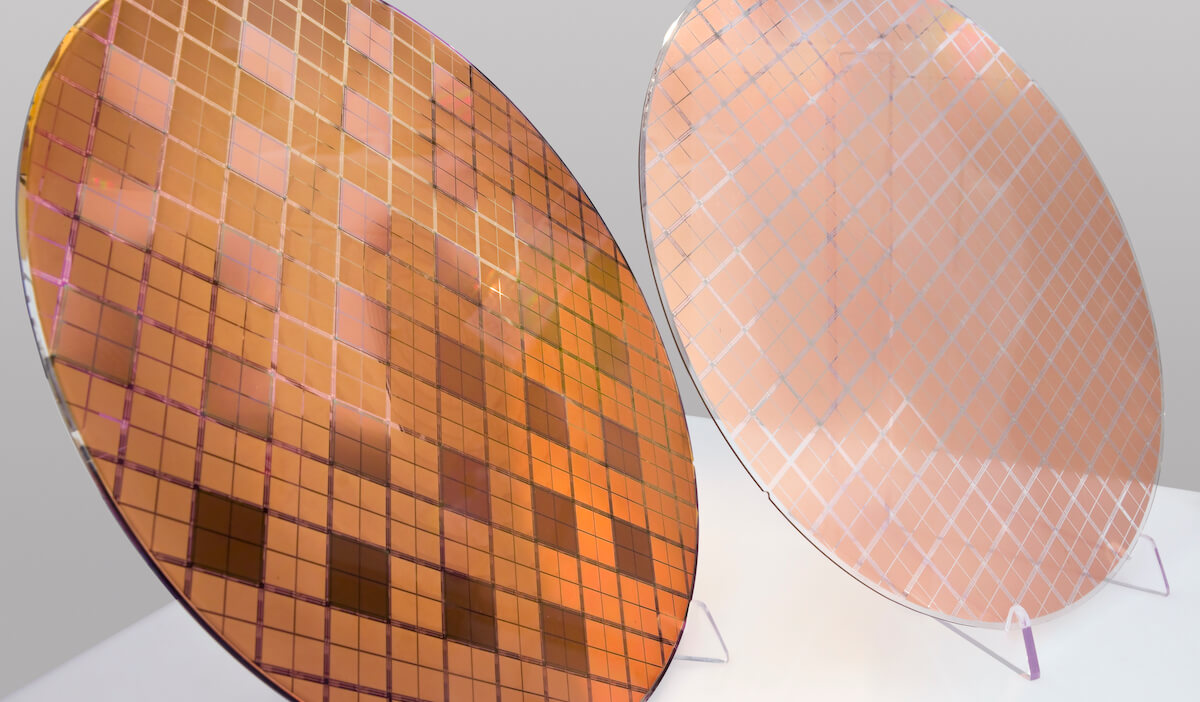
Absolics (SKC), announces glass substrates for semiconductor packaging
SKC ( a subsidiary of South Korean chaebol SK Group) has announced that they are building a 12,000 sq-meter, $80MM “semiconductor glass substrate” production plant in Covington Georgia by 2023 with plans to expand it to 72,000 sq-meter by 2025. This US subsidiary is named Absolics, and IFTLE is sure you will be hearing more about it in the months to come.
SKC’s Sung Jin Kim helped develop this glass substrate technology through research conducted at Georgia Tech Packaging Research Center while he was a research professor in the Electrical and Computer Engineering department at the Georgia Institute of Technology from 2012 to 2015.
Glass substrates reportedly allow the package thickness to be cut in half which will dramatically reduce power consumption. This would have a significant impact on data center footprints, which could be significantly reduced. Prototype packages reportedly “…have been certified technologically by a global semiconductor manufacturer”.
In general, ICs such as CPU or GPU, and memory are packaged as a module on a substrate together with several passive components such as multilayer capacitors (MLCC). In this SKC glass core solution, the MLCC can be mounted inside cavities in the glass core as shown in Figure 1.
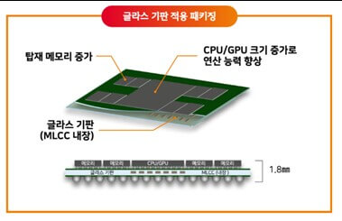
We can see that it is functioning as what we would call a BGA structure, which means it most certainly contains through glass vias and RDL on the surface. Their depiction also makes it look like some of today’s chiplet packaging structures and in fact it has been reported that SKC is proposing the use of its glass BGA substrates as an interposer for chiplet style packaging.
IFTLE will share more details as they are made available.
TSMC to Expand Packaging Production
Digitimes reports that TSMC is reportedly planning a new advanced packaging facility in southern Taiwan due to rapid increases in demand for 5/3/2nm chip manufacturing by customers such as Apple, AMD, Nvidia, MediaTek, and Xilinx.
This would be TSMC’s sixth advanced packaging plant. TSMC now operates (4) advanced packaging fabs mainly engaged in bumping, advanced testing, and backend 3D packaging. Hsinchu Science Park, Central Taiwan Science Park, Southern Taiwan Science Park, and Longton.
Its fifth packaging fab is now under construction at Chunan, has 1.3 times the aggregate of the existing four. The “mega plant” is slated for commercial production in the second half of 2022, focusing on 3D stacking.
Shortage of Engineers
So, you think you have an employee shortage? Nikkei Asia reports TSMC and MediaTek are looking to hire more than 10,000 engineers in 2022.
TSMC, with facilities being constructed in Taiwan, the U.S., Japan, and China expects to hire around 8,000 engineers in 2022. TSMC currently has more than 60,000 employees worldwide.

Fabless chipmaker MediaTek reportedly plans to hire 2,000 design engineers this year bringing its total number of employees to around 19,300. MediaTek hiring will be centered in Taiwan, though it is also looking to add a substantial number of new staff members to its R&D team in India, which currently has 1,000 employees.
To help maintain its lead in semiconductors, Taiwan recently opened new semiconductor graduate schools at four top universities reporting that it will invest ~ $11 million over the next 10 years to help bolster R&D talent within the domestic chip sector.
SHIP session at IMAPS DPC
Back in 2019, IFTLE asked the question “Is Advanced Packaging Production Returning to the US by SHIP?”
Other blogs have described Intel and Qorvo winning the digital and Rf segments of this Crane Navy SHIP [ SOTA Heterogeneous Integrated Packaging] program [link]
For those with an interest in this topic (and that should be any of you who read IFTLE) we want to point out the full session to be held at the Upcoming IMAPS Device Packaging Conf in early March.
The special IMAPS Global Business Council session entitled US Domestic Capabilities for On-Shoring of IC Packaging and Assembly for DoD Access will include these speakers:
- Darren Crum, Naval Surface Warfare Center, Crane Division – Technical Lead of the SHIP Program Director
- John Sotir, Intel Programmable Solutions Group
- Ted Jones, Qorvo, Sr. Product Line Director, Infrastructure and Defense Products (IDP)
- Tom Smelker, Mercury Systems – VP& GM
- Jeremy Adams, Micross Components – Vice President of Products & Services
- Brad Ferguson, SkyWater Technology – Sr. VP and Chief Government Affairs Officer
Hope to see you all at this can’t-miss session!
For all the latest in Advanced Packaging stay linked to IFTLE…………….

