
For the past few years, the ECTC committee has provided 3D InCites with a table outside the session rooms, rather than the technology corner, as part of our media trade. We consider it to be prime real estate, as pretty much everyone passes by the table at one time or another. People stopped by to chat; some just to ask where to find the registration desk, or the coffee, or in one instance, “are there any vending machines?”. The biggest advantage, however, is that I also get to talk to people who may not be exhibiting and learn about what’s happening at their companies.
Breakthroughs in glass
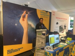
I caught up with Jim Haley, EMD Performance Materials, one of the co-authors of the paper, Design and Demonstration of Highly Miniaturized, Low-Cost Panel-Level Glass Package for MEMS Sensors, that won Corning’s Leadership in Glass Award. EMD’s contribution was the materials technology that enables low-cost interconnects in a glass substrate, explained Haley.
By using sintered copper (Cu) paste to form the through-glass interconnect, the team achieved the same results as Cu-filled through silicon vias (TSVs) at a much lower cost.
“One of the main technical challenges of working with glass is the metallization process,” noted Haley. “Sintered paste is a low-cost solution because it’s an additive process; you only put it where you need it, versus spraying or spin coating and etching away the excess. He said that in the 2D world, planar processes were the standard and worked fine. But now that we are dealing with 3D structures, additive processes will be the way to go.
Growing nanostructures
Speaking of additive processes, I also spoke with Vincent Desmaris, CTO, Smoltek, about the company’s latest achievement with its solid-state capacitor concept for heterogeneous integration systems that are under development.
By leveraging its core competency, growing nanostructures directly on a substrate, Demaris’ team has figured out how to replace traditionally integrated metal-insulator-metal (MIM) decoupling structures with a carbon nanofiber enhanced solution. Moreover, they achieved a technology breakthrough: a 5X capacitance/area improvement over their previous generation of solid-state capacitors.
The advantage for 3D packaging? This process allows decoupling capacitors to be placed as close to the chip as possible, explained Desmaris.
Start-ups to watch
Another breakthrough in glass technology that I learned about was from Shelby Nelson and Paul Ballentine of Mosaic Microsystems, a 3-month old start-up out of Rochester NY. Th company specializes in glass interposer technology and has worked out a way to support super-thin interposers in order to metalize through glass vias (TGVs). In a role reversal, the company’s proprietary temporary bonding process uses a silicon wafer as the carrier wafer and the glass interposer as the device substrate, rather than the other way around. Nelson reports good results with metalizing TGVs. Like EMD, the company has been working closely with Corning to develop low-cost glass interposer options.
Nirup Nagabandi, co-founder and staff scientist of Incendium Technologies was attending both ECTC and i-Therm. He talked to me about Incendium’s advanced stage thermal interface materials developed for high-performance computing (HPC) applications. These metal-based nanocomposite thin-films provide the cooling capacity of metals with the compliance of polymers. Nagabandi says this is a good solution for eliminating overheating issues on devices like mobile phones, PCs, microprocessors, LEDs, and energy storage devices.
Molecular Vista is a five-year-old startup based in San Jose, CA. According to sales director Robert Kertasaya, the company makes metrology and inspection systems that use infrared photo-induced force microscopy – or IR PiFM – to measure organic materials at the atomic level. These days, contaminants are so small, they’re almost impossible to identify, explained Kertsaya. The company is targeting both front and back-end wafer inspection, as well as package inspection.


From the Tech Corner
ASM Pacific Technologies sure has had a busy Q1: from Johann Weinhaendler, managing director, Amicra, I found out that the company has recently acquired both Amicra as well as Tel-Nexx Systems. Weinhaendler said the reason for the acquisition of Amicra is due to its die bonding capabilities for the photonics market, which is a sweet spot for Amicra, which now flies under the moniker, ASM-Amicra.
According to Weinhaendler, the company has achieved .3µm placement accuracy at speeds of up to 200 UPH with its Nova system. This meets market current requirements for Si photonics. The tool has also been qualified by customers for direct bond interconnect (DBI™) applications. Additionally, a high-volume manufacturing (HVM) version of the tool for DBI is in development.
“We have put more than five systems in the field in the last seven months at major OSATS and IDMs, mostly for Si photonics.” he reported.
Sustainable cleans
For the first time since its acquisition last August, Dynaloy was flying its new Versum Materials colors in the Technology Corner. I stopped by to visit Diane Scheele, business manager of the division. She explained that while Versum Materials has a history of strength advanced IC cleans, there was a gap in its product portfolio for wafer level packaging applications. Dynaloy fills that gap as it supplies formulated solutions for advanced packaging and wet clean processes. “Our chemistries and technology are complementary,” she said. “We can now provide any wet clean processes through the fab.”
Among other things, the company was showcasing its sustainable cleans. Scheele explained that the chemistries used to remove materials (adhesives, photoresists, etc.) for surface preparation and cleaning are very complex. Versum’s Green Chemistry check involves looking at traditional components in strip and etch processes and finding alternatives in their toolbox to reduce toxicity, extend lifetime and loading to minimize use, and reduce hazardous waste. The goal: making it easier for customers to comply with environmental regulations.
And that’s a wrap on our coverage of ECTC 2018. See you next month at SEMICON West. ~ FvT


