
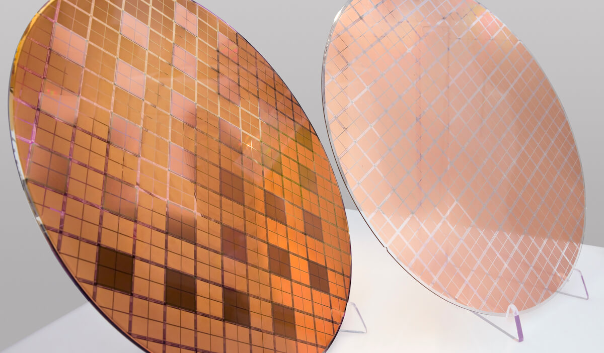
A number of research articles have been published over the past several years showing the advantages glass-based solutions can bring to packaging and systems integration including radio frequency (RF) front-end devices, interposers, MEMs devices, and integrated photonics. In particular, RF applications for glass are gaining interest for use as a substrate for filters, switches, and mm-Wave antenna arrays. The advantages include low insertion loss, as the frequency increases above a few GHz, relative to Si-based solutions; and higher integration density and much lower roughness compared to laminates and ceramics. Furthermore, we have seen numerous articles from universities, glass companies, and important members of the semiconductor supply chain (including TSMC, ASE, GlobalFoundries, and others) showing the successful demonstration of glass-based devices with impressive quality metrics, such as very low insertion loss compared with Si, demonstrated reliable performance and high Q-factors.
The question, is, with all of this interest and activity, why has glass not become more of a mainstream product? In fact, we heard from end-users at conferences in 2020 that through glass via (TGV) technology is still not ready. The biggest challenge, of course, has been maturing the supply chain to enable a smooth transition from small-scale demonstration to high volume manufacturing (HVM).
Mosaic Microsystems is changing this narrative with their handling solution that utilizes the Viaffirm™ bond and Si handle wafers. The approach uses a thin inorganic adhesion layer to temporarily bond a thin glass wafer (with or without TGV) to a silicon or glass handle wafer (Si handle wafer is the primary approach) (Figure 1). The thin glass substrate is then processed through downstream steps such as via fill, chemical mechanical planarization (CMP), redistribution layers (RDL)/passive deposition, lithography, and bumping. The key is that the bond is stable (remains temporary and does not outgas) to more than 400 °C. Utilizing a Si handle wafer allows the thin glass products to be fabricated leveraging existing equipment and processes, with only a mechanical de-bond that can be accomplished using existing solutions.
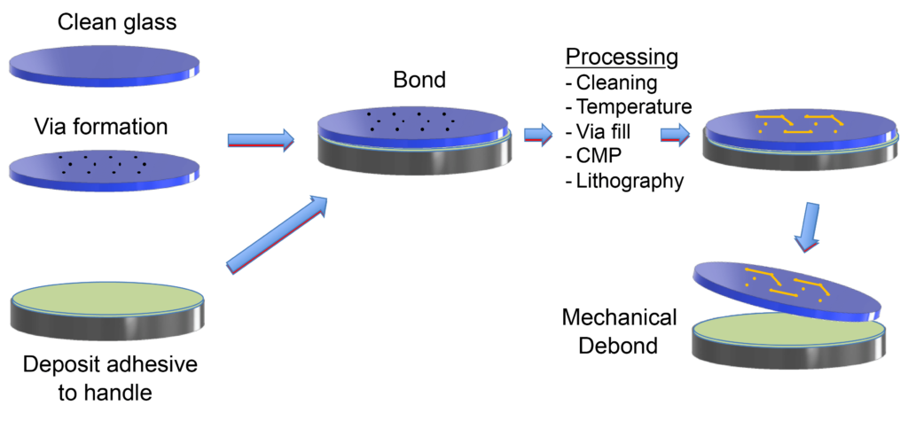
A key aspect of this handling solution is that it addresses the gaps in the supply chain that have hindered the adoption of glass-based solutions. It is important that this solution integrate seamlessly into typical back-end processes, which include via fill, CMP, RDL, de-bond, and dicing/singulation without significant changes or upgrades required of existing process equipment.
To achieve this integration, the strength of the bond is optimized to sufficiently enable downstream processing, but then be able to be de-bonded mechanically with low force. Depending on customer flow, this could take the form of transferring directly to dicing tape for die size dicing/singulation, transferring to another handle wafer for backside metallization, or permanently bonding to another wafer for further wafer-level packaging. Since the bond strength can be adjusted, this approach can also be used to create multi-wafer structures while also integrating passive devices, antenna, and/or switches as appropriate, making it attractive for incorporating glass in many potential products.
A key aspect of this process is that when the thin glass with TGV is temporarily bonded to the handle wafer, the vias look like blind vias similar to through-silicon vias (TSV). This allows you to plate the vias much like you would a TSV, which at this point is a mature process while avoiding the need for back-grinding and polish steps. This makes glass via fill readily available to the supply chain and is a step-change in the manufacturability of glass substrates. A good example of this is summarized in Figure 2. Wafer stacks with Corning Incorporated’s SG3 glass at 100µm thickness and TGV with 30µm top diameter were provided to Micross AIT for via metallization. The adhesion layer consisted of 100nm of Ti, followed by 300nm of Cu. Using their advanced plating chemistry, Micross was able to fully fill the vias in 100µm-thick glass, with only about 4µm of overburden on the surface.
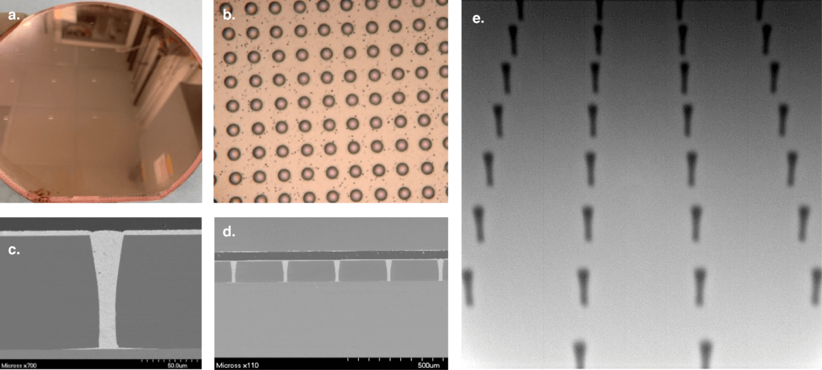
Figure 2a is a photograph of the wafer after plating, while Figure 2b shows the top view of the plated vias. The SEM cross-section image of a single via in Figure 2c shows the complete fill of the via. Figures 2d and 2e show the consistency of the fill, and no voids by cross-section and X-ray respectively.
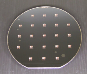
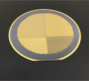
To achieve a via with good planarity, overburden often needs to be removed by CMP. Several bonded wafers were sent to Axus Technologies in Phoenix, AZ, for CMP. The wafer stacks were handled with the same conditions as for standard silicon wafers, and all polish runs completed successfully with no damage to the glass. Figure 3 shows an image of a metalized wafer post-CMP. All of these demonstrations were completed in the first lot of wafers, underscoring how well this approach ties into existing processes. Similar demonstrations have been done for plating/patterning

(Figure 4), de-bond, and multi-wafer stacking demonstrating suitability to leverage existing solutions to fabricate devices on glass <200 um thick.
SUMMARY
The material properties of glass make it an attractive material for next-generation applications, particularly in RF and heterogeneous packaging applications. For this reason, there has been a great deal of interest over the past decade to leverage glass solutions, but challenges to implementing these solutions in a high-volume environment have slowed adoption. This new temporary bonding technology provides a path for high volume implementation of thin glass solutions and represents a significant increase in the readiness for fabrication of glass-based devices.
This article first appeared in the 2020 Yearbook. Read the issue here.


Comments are closed.