
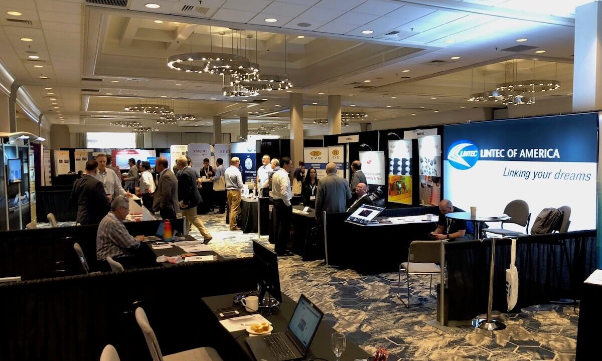
We hit the exhibits at IWLPC 2019 with a vengeance this year. Our mission was twofold – to find out the latest supplier offerings to support technology trends, and to spread the word about our new community membership opportunities on 3D InCites. But I’ll get to that part in a bit (or if your curiosity gets the better of you, scroll to the bottom.)
While we didn’t get to all the exhibitors (there were so many! 68 companies in all!), we did our best. There seemed to be an inordinately high number of exhibits at IWLPC focused on metrology and inspection. It’s a very hot topic right now, as advanced packaging is becoming more complex, and there is more at stake. Achieving high yields are critical to return-on-investment (ROI) in this segment of the semiconductor industry that is plagued with tight profit margins.
Breakthrough in Automated Inspection
The SVXR leadership was out in full force to promote its flagship tool. Co-founders, David Adler, and Scott Jewler were on hand to describe their high-resolution, automated X-ray inspection (HR AXI) tool, which is the first of its kind. It was developed as an alternative to automated optical inspection.
Adler contributed his front-end metrology and inspection expertise and Jewler provided his deep knowledge of advanced wafer-level packaging (AWLP) to design a transmissive inspection and metrology tool that brings front-end, fab-like inspection to advanced packaging.
Imaging speed and machine learning (ML) for defect detection with high enough reliability for an inline semiconductor application are two technology innovations that made SVXR’s 100X improvement possible, and until two years ago, it wasn’t available. We reported on this technology as part of IMAPS DPC coverage in March. You can also learn more about it here.
Consider the Source
From Canon ANELVA, comes a new X-ray source for non-destructive testing. This sealed transmissive microfocus X-ray source with a resolution of 2µm l/s at 6W uses diamond in the sealed tube to dissipate heat. It promises to be a game-changer, as it is the only X-ray source capable of capturing X-ray images with high resolution and high contrast simultaneously. Canon USA was also promoting its new wafer bonding tool with new technology that allows for room temperature bonding.
Acoustic Micro-imaging
Across the hallway from SVXR’s exhibit at IWLPC, Nordson SONOSCAN’s Steven Martell was promoting Sonolab, the world’s largest inspection service center specializing in acoustic micro imaging (AMI). It uses a waterfall-based system – rather than immersion – to run ultrasonic waves through the wafer to find defects,
AMI is ideal for finding cracks, voids, and misalignments in bonded wafer pairs. It is a complementary technology to X-ray – as X-ray doesn’t work on transparent materials. Used in tandem, they provide an optimum method of non-destructive inspection.
Finding Soft Defects
Lumina Instruments, a San Jose based start-up that launched at the beginning of the year, showcased its first product, the AT1 Thin Film Defect Optical Scanner. As VP Sales, Robert Kertayasa explained to me, there are two types of defects that can impact a device: hard particles and soft defects on thin-films and substrates such as scratches, water stains, bumps, etc. The AT1 is designed to find and map these soft defects on sub-nanometer thin film coatings on substrates.
“These are the defects nobody talks about. It’s a smaller market,” he explained. “Everybody else (the KLAs of the world) is looking for hard defects.”
Although it also works well on silicon, the tool’s unique contribution is scanning thin film on glass, which Kertayasa says is a growing market still in its infancy. Learn more about the AT1 here.
Speaking of Glass
My good friend, Terence Collier, Founder and CEO of CVInc. was holding down the fort in the next booth over from Lumina. I met Terence at my very first industry conference in 2005: the IMAPS International Symposium in Philadelphia. He knows pretty much all there is to know about wafer bumping and was a regular contributor to Advanced Packaging Magazine.
Collier confirmed that glass substrates are gaining traction because it’s possible to achieve tighter pitches and higher density vias in glass than in silicon. Thermal stress creates a problem for silicon, he explained. Collier’s team has been working with glass substrates for some time, in particular, putting through glass vias (TGVs) in glass interposers.

Glass interposers are ideal for RF and optical applications, he said. At CVInc, they’ve achieved TGVs and filled vias that are 30um diameter, 50um pitch, and 480um tall, reaching aspect ratios of 40:1. They’ve also formed redistribution layers (RDL), metalizing both top and bottom layers, to allow integration of active and passive devices.
Not much further down the hall, Plan-Optik was showcasing its portfolio of fused glass and silica patterned wafers for numerous MEMS applications, such as capping and as substrates, as well as TGV wafers and carrier wafers for temporary bond/debonding. One of the wafers on display had a special honeycomb pattern designed for a temporary bond process that uses thermal release adhesive. The company has some new breakthrough technology that will be revealed next week at SEMICON Europa. So, stay tuned for more on that.
Filling a Need for Small Outline Packages
While the big OSATS are focusing on next-generation, high-density advanced packages, they are creating a gap for small-outline packages, for which there is still a need, according to Sam Gomez, STARS Microelectronics.
Automotive and medical are growing markets calling for an increasing number of customized components. As we heard during the fan-out panel-level packaging discussion, the only wafer-level chip-scale packages used in automotive are for infotainment systems, and the only fan-out packages are used for 77GHz radar. The remainder of the growing automotive content is more traditional packages used for MEMS and sensor integration. This is the niche being filled by STARS. “There are a wide variety of applications requiring small packages with low pin counts,” he explained, calling them “jellybean” type packages.
The Changing EDA Landscape
We stopped by to visit with Bill Acito, Cadence. It’s always great to see EDA vendors exhibiting at a conference. Acito was one of two Cadence presenters in the design session. Mentor also presented. While Zuken exhibited, they did not present. All three companies were contenders in last year’s 3D InCites Awards.
These companies clearly get it, and I applaud them for endeavoring to educate packaging engineers on the importance of EDA, especially as system-in-package (SiP) and particularly chiplet integration drive the need for system planning and aggregation upfront.
“The blurred line between the IC and the package is gone,” says Acito. “SiP is becoming the new SoC. It isn’t about IC or IC manufacturing processes. It’s about leveraging capabilities in both design spaces. EDA vendors need to support this.” I wish the packaging engineers would too, but by the looks of the sparsely attended session, there’s still lots of education that need to happen.
Final Tidbits from the Exhibits at IWLPC
I spent some time with NXQ CEO, Lenore Arnold, talking about some new things that are in the works, but we can’t quite talk about them yet. NXQ is currently known for its mask alignment technology that allows for capturing a pattern in one shot, without needing to stitch anything together, she explains. This is due to smart alignment algorithms.
Suffice it to say that the company is “expanding its tool offering, leveraging the optics technology that set its mask aligners apart from the competition. All I can say is, the new tool is not a mask aligner. It’s something “that many people need more than the need mask aligners,” said Arnold. Stay tuned for the big reveal in the next few months.
And finally, over at the SUSS Booth, Todd Schivo reported that the company is back in the permanent bonding business. “Things are sticking together well,” he said. And contrary to popular belief, they never left the temporary bonding/debonding business. I hope to get more details next week at SEMICON Europa.
3D InCites Community Memberships Coming in 2020
We have some of our own exciting news to share. 3D InCites is in the process of a redesign that puts the emphasis on the community we have built over the past 10 years. Your annual $1000 investment in a community membership will allow us to continue bringing you the event coverage (like this) that you’ve come to rely on. We’ve priced it low, to fit into all your budgets. You’ll also get some great perks as part of your membership, including your logo on our home page, participation in weekly member spotlight, a 10% discount on advertising, and much more. For details, download our 2020 3D InCites Media Kit here.


