
Qorvo Begins SHIP RF Packaging Program
IFTLE has previously discussed the US State-of-the-art Heterogeneous Packaging and Prototyping (SHIPS) program (see IFTLE 422 “Is Advanced Packaging and Production returning to the US by SHIP?”)
Qorvo was among the phase one winners in the SHIP program along with Intel, Xilinx, Northrop Grumman, GE, and Keysight Technologies.
The SHIP program is split into digital and RF tracks. Intel won the digital contract. In November it was announced that Qorvo had been selected to create a SHIP RF packaging production and prototyping center.
The agreement is worth up to $75M. The monies will reportedly be used to expand the capability and capacity of Qorvo’s Advanced Microwave Module Assembly (AMMA) in Richardson, Texas. Qorvo is currently a $3B company whose revenue contribution is about 80 percent commercial and 20 percent defense.
Under the SHIP program, Qorvo will design and deliver state-of-the-art heterogeneous packaging integration, which has been deemed essential to meet the size, weight, power, and cost requirements for next-generation phased array radar systems, unmanned vehicles, electronic warfare platforms, and satellite communications.
Qorvo will reportedly use the financial support to enable or accelerate these initiatives:
- Increased automation for assembly tools
- Expanded technology offerings
- Research into new packaging types – 2.5 and 3D
- Development of foundry models.
Qorvo holds a Defense Microelectronics Activity (DMEA) Category 1A trusted source certification for package assembly, test and wafer foundry services at the Richardson, TX location.
SEMI Developing Panel Level Packaging Standards
Earlier this month, SEMI revealed some of the highlights of the activity of the 3DP&I Japan Technical Committee (TC) as they develop panel level processing standards. This task force (TF) kicked off in October 2019 and plan to submit a ballot in 2021.
Encapsulation Materials
Several types of encapsulation materials are used for WLP and PLP including granule, sheet, and liquid type. The encapsulation process varies based on the encapsulation materials. Mold resin material characteristics are specified for legacy packages such as leadframe and BGA packages, but there is no specification for encapsulation characteristics for FOWLP and PLP.

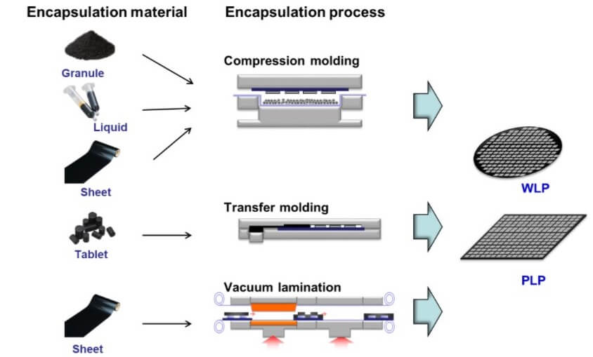
Figure 1: Encapsulation materials and processes.
The committee has been developing measurement/testing methods for key mold compound material characteristics such as wettability, gel time, CTE, Tg, flowability, modulus, viscosity, and shear strength.
Warpage and TTV
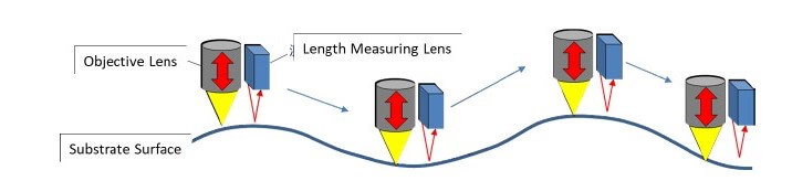
This committee is also working on the development of PLP panel warpage and total thickness variation (TTV) measurement methods. In order to minimize line width, it is necessary to reduce the depth of focus of the exposure beam as the exposure beam NA increases. For instance, when the target line width is 1 µm, lens NA0.4 is required, and the depth of focus is 2 µm. So, the measurement metrology is a key to understand the encapsulated panel surface roughness, warpage, and TTV to achieve finer RDL.
Glass Carrier Specifications
The specification items are as follows:
- Substrate size, thickness, edge condition, squareness, surface roughness, warp, TTV
- Orientation corner
- ID mark location
For further information contact Mami Nakajo/SEMI Japan
And now the IFTLE family wishes all our readers Merry Christmas and a Happy New Year!