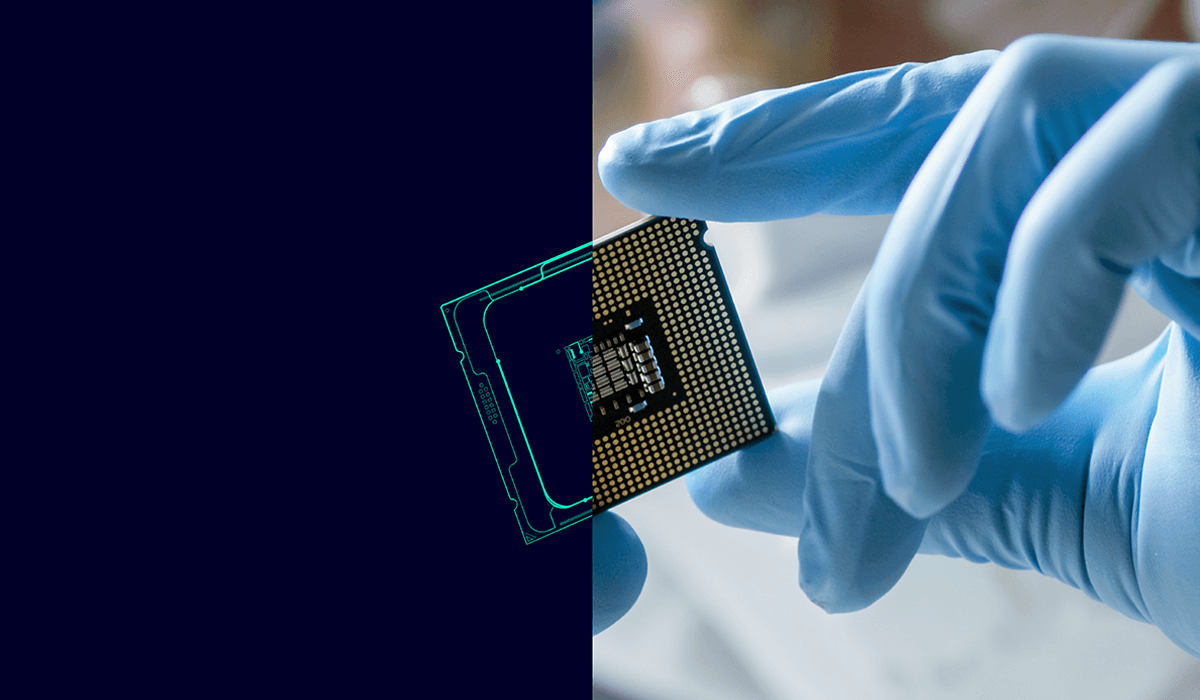
Numerous package designers possess extensive hands-on experience in crafting organic FR4/HDI build-up BGA/LGA substrates. They have mastered the design guidelines, and the fabrication of substrates is thoroughly familiar to them. Proficient in utilizing design tools like precision scalpels, these designers efficiently complete projects within specified timelines, meeting specifications, and budget constraints. Whether it involves flip-chip attachment, wire bonding, or a stacked die combination, the design methodology is comprehensively understood.
Then, management introduces the concept that the upcoming generation of designs will involve heterogeneous integration, incorporating new platforms such as RDL-based fan-out wafer level packaging (FOWLP) and/or interposers. Suddenly, you find yourself transitioning to FOWLP and 2.5D design. Discussions shift to terms like assembly design kits, stream-out, sign-off using Process Design Kits (PDKs), multi-pass degassing, seal rings, assembly layout vs. schematic (LVS), and High Bandwidth Memory (HBM) stack routing.
The idea is floated that new design tools might be necessary—semiconductor place-and-route tools that exclusively operate on Linux and are entirely script-driven with TCL/TK. As individuals delve into online research and attend conferences, listening to EDA tool vendors, they might find themselves at a crossroads, wondering: Am I becoming obsolete? Do I really need to familiarize myself with silicon place-and-route tools? What does assembly LVS entail? Why the need for multiple pass degassing? And what’s the rationale behind hatching and offsetting my metal planes?
The technological shift can indeed be daunting for many of us. However, there’s no need to despair. While there is a host of new terminologies to grasp and numerous design techniques to comprehend and master, along with an entirely new design process and flow, the good news is that overcoming these challenges doesn’t necessarily require learning silicon place-and-route design tools.
We have unmistakably transitioned into a design realm where the traditional distinction between silicon die design and IC packaging design is no longer clearly defined. In this evolving landscape, silicon foundries are producing substrates, and OSATs are incorporating silicon as a substrate material, causing a convergence of these two design domains. This prompts the question: Can IC packaging design tools be effectively employed for the design of silicon substrates?

The IC packaging design tool set has reached a level of maturity enabling it to cater to a wide range of substrates, including classic plastic, organic, and ceramic packaging, as well as silicon substrates driven by interposer and chiplet designs. Importantly, in most cases, system and packaging teams are not required to forsake their current toolset to accommodate these designs. In fact, the packaging design toolset can provide added capabilities, particularly in the realms of multi-component system design and component stacking, surpassing the capabilities of an IC layout tool.
In this Siemens white paper, An Organic Package Designer’s Guide For Transitioning to FOWLP and 2.5D Design, we share insights based on the experiences of organic package substrate designers who have transitioned and mastered RDL-based FOWLP and 2.5D silicon and organic interposer design, while still using (and preserving) the majority of their existing packaged design tools and skills.