
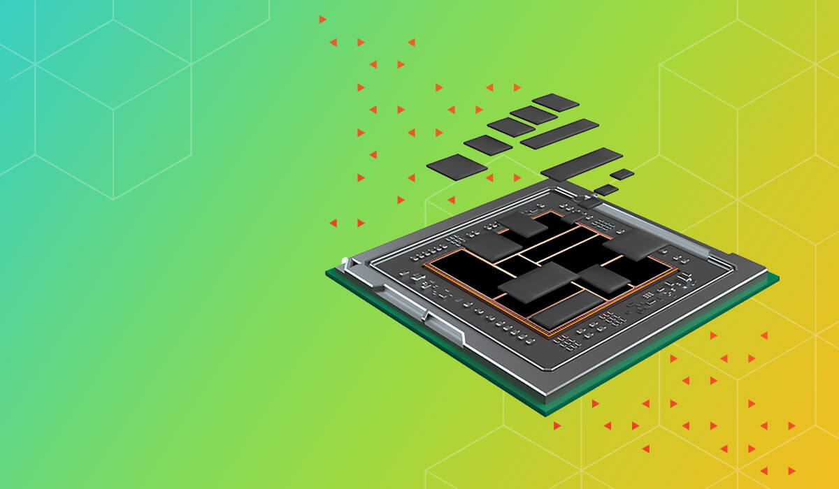
In electronic product design, solely relying on process shrink as the primary driver of product innovation and improved system performance is no longer a viable approach. The cost and complexity associated with advanced nodes have everyone looking for alternatives to the traditional monolithic system-on-chip (SoC). The path most is taking leads to the world of “More than Moore” and heterogeneous integration. These heterogeneous, multi-chiplet architectures provide a much lower cost alternative to the latest design nodes, while still providing a robust reuse model based on IP in the form of physically realized chiplets. The package design now sits in the center of the universe for the next generation of electronics.
One of the primary challenges designers face during the transition from monolithic devices to multi-chiplet architectures is the planning, management, and optimization of top-level design and connectivity. To address this challenge, a novel system-level design management platform is needed to aggregate data from IC designers, package designers, and board designers. This platform facilitates system-level optimization and provides the top-level netlist for connectivity verification.
Traditional package designers also face challenges in adapting from layout expertise in laminate substrates to silicon substrates. Using silicon substrates also requires a formal physical verification process that may be unfamiliar to many package designers. Additionally, electrical and thermal analysis pose significant challenges in the design process. The tools employed for these analyses must support system-level considerations and account for on-chip and off-chip devices, interconnects, and cross-domain coupling effects.
The semiconductor packaging industry is now poised to take on a more prominent, more significant role in the electronic product design of the future. To meet the market demand for these heterogenous, chiplet-based architectures, new system-level design methodologies are required, targeting system-level power, performance, and area (PPA). In this white paper, we highlight the evolving role of semiconductor packaging in electronic product design, specifically in the context of heterogeneous architectures and chiplet-based systems. With the increasing market demand for these advanced designs, new system-level design methodologies are necessary to optimize PPA at the system level.


