

Technology innovations don’t reach customers right away. Since 1980 I have observed how our industry has improved key parameters like cost per function, power dissipation, form-factor, complexity and clock-speed by many orders of magnitude. However, every new technology took at least several years, sometimes more than a decade, until it proliferated beyond a very small group of power users and a narrow range of applications. Key reasons for these delays were, and still are, high initial development and unit cost, as well as the challenging and time-consuming efforts needed to transform a new and innovative technology into high-value, customer-specific solutions.
ASIC to the Rescue
In the 1980s and ‘90s, ASIC Design Centers allowed companies like IBM, LSI Logic, NEC, TI, Toshiba, and VLSI Technology to work with/for customers to develop unique and application-specific integrated circuits (ASICs). They accelerated market acceptance of internally developed technology and transformed it into customer-specific solutions.
Since ~ 2000, companies like Broadcom, Nvidia, Qualcomm, and other fabless IC vendors have utilized ASIC design methodology to combine innovative proprietary and third-party hard and/or soft IP building blocks (a.k.a. “Semiconductor IP”) to compose ASICs. They complement these ICs with engineering advice, software and additional active or passive components, at the board-level. As was clearly conveyed in most SEMICON West 2019 keynotes, several Heterogeneous Integration Roadmap (HIR) sessions and at the Test Vision Symposium, more of these customer-specific solutions are being integrated into advanced packages, to bring up customer-specific, (sub)system solutions faster and at a lower cost.
Value Creation Shifts from Die to the Package
Today, more applications are becoming too complex and/or require a large portion of heterogeneous functions and therefore can no longer be integrated in a single-die. Advanced packaging technologies enable the integration of multiple, die-level building blocks (a.k.a. chiplets) in one IC package, and shift a significant part of a design’s value creation from the die to the package.
Utilizing the latest feature sizes for digital logic, integrating large amounts of memory, and using specialty process technologies for analog, RF, optical, MEMS as well as other functions, expands the range of development challenges significantly. This suggests engaging with experienced partners to reduce risk and assure that the project stays within budget and on schedule, from design start, through design bring-up to volume production.
“Real men” have fabs?
Just like the phrase, “Real men have fabs” didn’t stand the test of time, nor did the implied gender bias. Relying on internal resources only is very risky in today’s fast-moving and highly complex semiconductor industry. Allow me to transform this famous quote into “Visionary executives have competent partners”. I learned the importance of the latter quote the hard way, because two of my previous employers failed, primarily because top management didn’t want to invest in third-party ASIC design tools, nor in building a cost-effective manufacturing supply chain.
A Competent Partner and General Contractor
Finding all the right partners, for all the complex design and manufacturing steps is difficult, costly and time-consuming. Allow me to suggest engaging one experienced partner as a general contractor. This company can engage and manage all the competent subcontractors you need for IC or (sub)system development and production.
eSilicon is one such partner, with an excellent track record of developing customer-specific solutions. This Silicon Valley fabless ASIC company captures a customer’s requirements, then complements latest merchant design capabilities with its own innovations and expertise to develop and bring up a customer-specific solution. They also understand how to best utilize the capabilities of powerful manufacturing partners to ramp up IC production. In addition, they can manage the entire supply chain through a product’s lifecycle. If given the opportunity, they’ll cost-reduce a proven design to extend its life and/or carry essential building blocks forward to the next-generation design.
High-density Advanced Packaging (HDAP) Challenges
As more and more of the value creation is shifting from the die to the package, understanding and solving single and multi-die HDAP-specific challenges becomes an important success criterion. The proximity of HDAP building blocks (multiple dice, interposer(s), package substrate, intra-package connections, passives, over-mold, …) demands to analyze the electrical, thermal, thermal-mechanical and magnetic characteristics and interactions of all these building blocks, to meet performance, cost and reliability goals. Unlike in the past, when adding plenty of design margin was acceptable, today’s complexities and unit cost pressures do not allow this approach anymore. Likewise, today’s time-to-market pressures don’t allow multiple design iterations until a prototype comes “close enough” to the customer’s requirements.
Electronic Design Automation (EDA) Partners’ Contributions
EDA tools have enabled our industry to grow from 500-gate ICs that I marketed in 1983, to billions of gates today. EDA tools remain mandatory for managing today’s die-package-board-system designs and for analyzing the rapidly increasing multi-physics design challenges. However, no EDA vendor can offer a complete design solution yet. A designer needs to evaluate the available point tools, choose the best-in-class tools for parameter extraction/model generation, design planning, implementation, verification as well as test program development, then combine them into a die-package-board-system design flow for their specific application.

Outsourced Semiconductor Assembly and Test Partners’ (OSATs) Contributions
Just like the design of a die can’t start without a process design kit (PDK), advanced package designers can’t start their work without a package assembly design kit (PADK) that contains technical details about the OSATs’ available package types, assembly and test capabilities, characteristics of materials used and design rules that assure swift production ramp-up and good yields in volume production.
A real-life example for today’s challenging high-speed, multi-dice designs
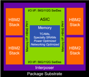 eSilicon’s highly configurable FinFET-class 7nm IP platform, illustrated below, includes the technology to create an application-optimized processor core with four high-bandwidth memory (HBM) stacks. eSilicon can then integrate them side-by-side on a silicon interposer – a complex example for a 2.5D design in an advanced IC package.
A recent white paper from ANSYS entitled “Speeding 5G Network Infrastructure Design” details how eSilicon used ANSYS multi-physics tools to perform chip/package/system design on an advanced 5G infrastructure ASIC. Highlights of the story include:
- eSilicon use of HFSS and SIwave to perform 3D extraction and to generate S-Parameter models for the silicon interposer and package substrate design. They used these models to analyze how interconnect geometries and material characteristics affect signal integrity (SI) in the frequency domain. eSilicon also analyzed the insertion loss, return loss and crosstalk performance of the high-speed interconnect.
- eSilicon’s engineering team concatenated S-parameter models of the interposer and substrate to form a complete package model and provided it to the customer for their IBIS-AMI channel analysis to verify system-level transmitter and receiver performance in the time domain.
- To analyze DC and AC power integrity (PI), eSilicon used both SIwave and RedHawk to model the power distribution network (PDN) between the voltage regulator module (VRM) on the PCB and through the substrate, interposer, and die, including all capacitors.
- For the final verification step of the 5G design, eSilicon worked with ANSYS on a chip-package-system (CPS) power integrity analysis flow that models each component in the system. In addition to verifying the IR drop and self-induced noise performance, this flow enables further design optimization by showing how the different components interact with each other.
With regard to the all-important semiconductor intellectual property (IP) aspect of advanced chip design, eSilicon relies on its IP partners for mainstream, standards-based IP, such as PCIe, DDR, and USB. For mission-critical IP, such as HBM PHYs, advanced memories, and SerDes functions, eSilicon develops these IP blocks internally to ensure the highest performance and lowest power capabilities will be available when their customers require it.
Summary
If you ever have significantly remodeled your home or built a new one, you’ll appreciate the role of the general contractor. He/she manages masons, carpenters, plumbers, electricians, painters, roofers, etc. to complete their high-quality work on your home on time and within budget.
You may want to consider eSilicon as a general contractor for your next multi-billion gate design. ~ Herb


