Keeping pace with Moore’s law continues to be challenging and is driving the adoption of innovative packaging technologies that support continued system scaling while doing so at lower costs than comparable monolithic devices.
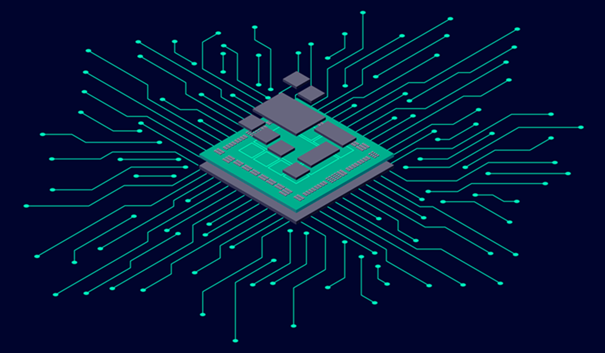
These packaging technologies disaggregate what would typically be a homogenous, monolithic device — like an ASIC or system-on-chip (SoC) — into discrete, unpackaged dies, known as chiplets, specifically designed and optimized for operation within a package in conjunction with other chiplets (Figure 1). This is also referred to as heterogeneous integration (HI), where multiple dies or chiplets for 2.5D/3D are integrated into a system-in-package (SiP) design.
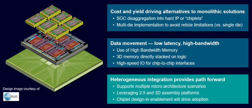
Heterogeneously integrated SiP devices offer considerable benefits, including higher performance, lower power usage, smaller area, lower cost, and faster time to market. However, thus far they are designed and produced by only a small number of advanced users. Broad industry proliferation will require a standardization of chiplet models and die-to-die connectivity IP—efforts currently underway—supported by new workflows.
This article will focus on five workflows that are essential for planning, implementing, verifying, and co-designing heterogeneous design of chiplets for 2.5D/3D. (Figure 2).
- Architectural planning and analysis
- Physical design planning and analysis
- Design analysis
- Reliability analysis
- Test planning and validation
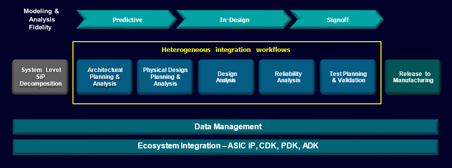
As a design moves through the five workflows, it also undergoes modeling and analysis to continuously qualify that the design meets its performance specifications.
Predictive modeling is applied during the architectural and physical design planning phases, with the primary goal of qualifying engineering decisions and gaining insight into downstream performance. This also enables team members to validate their packaging and system architecture selection to best address the problems they are trying to solve.
In-design modeling further qualifies a design as more content and details become available during implementation. The objective is to identify and resolve issues while corrective action is still relatively easy and inexpensive. These issues are typically related to power, thermal, signal integrity, process rules, or even mechanical integration.
The last step is the final signoff of the completed design before release to manufacturing. Because HI designs include a wide range of multi-domain design content and IP, comprehensive data management support throughout all five workflows is required.
Now let’s look at the five workflows themselves in a little more detail.
Architectural Planning and Analysis
The architectural planning and analysis workflow enables system and RTL designers to rapidly explore and capture viable design architectures leveraging three key inputs:
- The chiplet components and corresponding design kits
- Standard high-speed protocols for internal die-to-die interfaces within the package
- External chip-to-chip interfaces between the SiP package and other chips within the system at the PCB level
These high-speed interfaces can be captured using a library of generic connectivity IP models and then mapped to alternate vendor-specific and technology-specific connectivity IPs. This enables the system designer to assess the power, performance, area, and cost attributes of various scenarios against the system requirements.
In this way, predictive modeling helps engineers to hone in on the optimal micro-architecture through the identification of a finite set of scenarios, or micro-architectures, and the exploration of multiple configurations, and partitioning scenarios.
Physical Design Planning and Analysis
Once an optimal SiP architecture is identified, detailed design can begin, including physical planning, implementation, and analysis.
The physical design planning and analysis workflow applies to both interposers and package substrates. It encompasses package floor planning, IO planning, power delivery, substrate route feasibility, and netlist optimization, along with the corresponding checks, such as LVS and LEC.
Predictive modeling is used during floorplanning and implementation to continuously qualify the design, which ultimately streamlines the design process. As detailed design structures, like power planes, get implemented, the modeling fidelity and quality of results will improve.
As co-design of one or more custom chiplets is fundamental, tight collaboration between the silicon and package design teams must be fully supported. This means establishing robust multi-domain design data management along with comprehensive engineering change order support to facilitate the exchange of data between teams and disciplines.
Design Analysis
The design analysis workflow incorporates extraction and simulation tools that support analysis of SiP signal and power integrity, static and dynamic IR drop, electromigration, and timing.

Traditional signal integrity techniques can be used to simulate the high-speed interfaces. Static timing analysis is required for the low-speed signals and the test and control type connections.
The power integrity approach taken must be adapted to account for multi-chiplet scenarios. These structures require detailed parasitic extraction that supports both silicon and organic substrates as well as combined SiP and die level extraction for IR drop and electromagnetic analysis.
Reliability Analysis
Two key areas that require extensive reliability analysis are thermal and mechanical stress. Given the proximity of devices in HI designs, there’s a high likelihood of some type of chip-to-chip or chip-to-package interaction. Therefore, thermal coupling can be a big concern.
This intensive level of analysis requires detailed thermal chip models. The models need to account for power density and transistor level heating at the die level, and assuming uniform temperature across the die is no longer realistic.
Mechanical stress can also be an issue given the substrate size and different materials used. For example, with a large, multi-reticle silicon interposer sitting on an organic package substrate, the analysis must account for different coefficients of thermal expansion values and must evaluate effects like thermally induced bump stress or substrate warpage.
Design for manufacturing and electrical rule checks also need to be performed at both the chiplet and SiP levels. These include checks for electromigration, electrostatic discharge, latch-up, and electrical over-stress. To expedite this type of SiP analysis, the required chiplet models and performance data should be included in their respective design kits.
Test Planning and Validation
Perhaps one of the more challenging workflows for HI is manufacturing test, as it requires design for test (DFT) infrastructure, wafer-level test, die test in package, and interface testing between the dies.
The good news is that there are established DFT standards for testing 2.5D and 3D designs, including IEEE standards 1838, 1687, and 1149.1. Additionally, this workflow is supported by recent DFT advancements like memory testing and built-in self-test (MBIST) with 1838 compliant test access ports; scan testing that supports a 3D package pattern retargeting flow; and die-to-die interconnect testing using differential wearing scheme chains composed of wrapper cells. These methods must be designed early to support SiP testing; this requires planning at the package level for probe pad access and test IO—similar to planning requirements for high-speed IOs.
As well, it is imperative to understand that test considerations cannot wait until the end of the design flow and must also be incorporated into early planning. Packaging engineers must collaborate with test engineers to develop the test IO plan and support static timing analysis and timing simulation requirements.
Multi-Domain Co-Design Unlocks the Benefits of HI
Successful delivery of heterogeneously integrated systems requires integrated, multi-domain workflows and collaborative design methods throughout the entire design lifecycle.
Heterogeneous design generates a tremendous amount of multi-domain data spanning the entire product lifecycle. This necessitates managing a design database for the system, RTL, silicon, and even mechanical design. HI design also includes a broad spectrum of IP, materials, and design kits. All this data needs to be carefully managed and synchronized to ensure efficiency and design integrity throughout the design process.
There are numerous advantages and benefits of heterogeneous integration. It enables larger, more complex systems than monolithic SoCs and offers improved power, performance, area, and form factors. However, these benefits do not come for free. There are key challenges that must be met, including optimal decomposition and architecture selection, power delivery through the system, as well as thermal management, timing, and test. Companies that want to overcome the challenges and reap the full benefits of HI design should focus their efforts on building, qualifying, and deploying the five workflows presented in this article.
This article first appeared in the 2024 3D InCites Yearbook. Read the full issue here.