
Editor’s Note: Bob Smith, executive director of the ESD Alliance, a SEMI Technology Community, is a regular contributor to 3D InCites. He turns over his blog today to John Lee of Ansys, an ESD Alliance member company, who describes a disruptive change in product engineering and the requirements of the new 3D world that requires 3D-IC designs.
The growing adoption of 2.5D and 3D integrated circuits (3D-ICs) marks a major inflection point in the world of semiconductor design. Driven by the pervasive use of AI/ML, 5G/6G networks, and autonomous vehicles, electronic designers demand greater integration densities and faster data transfer rates that have outpaced the capabilities of any single chip. 3D-IC technologies provide a solution embraced by leading-edge system design companies and are increasingly supported by semiconductor manufacturers.
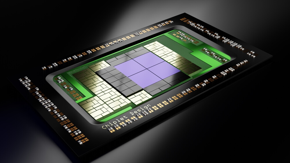
3D-IC is an umbrella name for a range of manufacturing technologies that enable the integration of multiple silicon dies into a single package. The dice, also referred to as chiplets, can be placed closely on a connectivity substrate (2.5D) or stacked vertically on top of each other (3D). 3D-ICs offer many advantages over SoCs. They:
- Circumvent reticle limits that define the maximum size of a single die.
- Provide faster signal speeds at lower power than traditional packages on printed circuit boards (PCB).
- Improve system performance by stacking memory chips on top of the logic that accesses it, reducing delays.
- Make it possible to use a mix of different silicon process technologies in one system.
That’s the good news. To capture these benefits and achieve a competitive advantage, designers face serious technical and organizational challenges. The principal issue is that 3D-IC designs blur the lines between three traditionally separate design disciplines: chip design, package design, and board design. These three design teams draw on different design tools, different data formats, different terminology, and different manufacturing knowledge bases. Now suddenly, 3D-IC is smashing them all together into a novel design challenge with significant contributions required from all three. A fundamental, disruptive change is coming to how product engineering is organized, and the brew of competencies required to succeed in this new 3D world.
3D-IC Designs Blur the Worlds of Chip, Package, and Board
Today, the package design team is typically separate and distinct from the chip design team with only limited communication between the two. That all changes when the design spans multiple dice and the packaging become an integral part of the system. Indeed, if logic blocks are dispersed across two or more dies, they communicate through wiring contained in the package substrate or interposer layer, meaning the design of that package is no longer separate from the design and floor planning of the chip. Chiplets stacked vertically on top of other chiplets connected through direct micro bump contacts, further complicate the distinction between the package and die.
The blurring is further exacerbated when we consider the interconnect routing on a large 3D-IC substrate. It is a complex mixture of chip and board strategies like non-Manhattan routing, river routing, and electromagnetic modeling. Each 3D manufacturing technology is different, but they typically erase the notion of an easy separation between PCB design techniques and chip design techniques.
What does this blurring of the lines mean for semiconductor development teams? It means they will have to adapt to accommodate three major change areas:
- There is a cultural/organizational challenge as cross-functional and interdisciplinary experts must now work together as a close-knit team to bring 3D-IC designs to market. Designers must now collaborate more closely than ever, mastering the art of the board, package, and silicon simultaneously. The usual, siloed organization of design teams will have to be rethought. Silos must be eliminated so that collaboration can flourish.
- Traditional EDA tools do not support the advanced technical design requirements of the 3D-IC design. A new generation of purpose-built tools is emerging that offer essential new capabilities like multi-die 3D floor planning. The expanded range of physical effects impacting the design is driving the need for open, flexible, extensible, and high-capacity design platforms. These new platforms must accommodate the broad array of analysis and design tools needed to solve the multitude of 3D-IC design challenges. No one tool addresses all the issues. And the huge capacity demands of these giant 3D systems make cloud computing essential. Closed single-company design systems won’t cut it!
- Multiphysics analysis is already a fact for advanced node design and is a necessity for 3D-IC. Designers need to consider a range of novel physics challenges, many of which they never had to deal with before. Multiphysics is not the same as multiple physics – these physics interact in a non-linear fashion and need to be analyzed concurrently. 3D-IC teams will need to master new design constraints. Chief among these is the need for thermal analysis at every step of the design flow. Power dissipation is one of the primary limiting factors of 3D-IC design and careful analysis is essential for a reliable working device. Mechanical aspects related to package stress and warpage also must be considered upfront starting with the floor planning stage where the unfortunate placement of hot and cold components can doom the design from the outset. Other unfamiliar effects can come to the fore with distributed systems, like low-frequency power supply oscillations between components on the substrate. Concurrent multi-physics, not just multiple physics!
Managing Organizational Change for 3D-IC Success
The pioneers in 3D-IC design have mainly been large corporations with deep resources that benefit from a vertically integrated culture and organizational model that enables interdisciplinary collaboration, and results in stunningly advanced bespoke silicon. Other early adopters are start-up companies in the AI/ML field and similar that have organized themselves with 3D-IC in mind from the get-go. More mainstream, horizontally integrated companies can be challenged to achieve the level of teamwork, synergy, and expertise needed to optimize a 3D-IC design.

My experience working with Ansys customers leads me to believe the answer lies in creating a team environment with an open design platform that pulls together designers from different groups with the range of expertise required to address 3D-IC. Realistically, not every designer can be an expert in the full range of physics that impact these systems, so it is essential to arm them with design tools and multi-physics analysis tools that automate the analysis as much as possible. A good analysis tool encapsulates the required expertise, making it available to designers through easy-to-understand outputs.
This kind of ecosystem provides a powerful advantage in focusing the entire, cross-functional team on a shared, real-time view of the product design — and driving the innovation that leads to success in today’s competitive worldwide semiconductor industry.
A good place to learn more about the state-of-the-art in multi-physics and 3D-IC design is the recent Ansys IDEAS Digital Forum, now available on-demand.


