As the power density increases for semiconductor devices, thermal management is becoming an ever more critical challenge for reliability and performance, for high-performance computing, AI, data center, power electronics, and other applications. Heat dissipation is often a great concern as the junction temperature rises with an increased power density, which can adversely affect the performance and reliability of the semiconductor device. This is even more complex and challenging for heterogenous integration, with multiple chips of various functionalities, sizes, and power distributions, and the attendant thermal performance requirements – all in the same package.
For this purpose, various thermal management solutions have been under development in the industry and academia. Novel thermal interface materials (TIM), such as phase change materials (PCM), liquid metal alloys, graphene, graphite, and composite materials, have been developed for high thermal conductivity and low thermal resistance. Cooling solutions, including heat spreaders, heat sinks, and heat pipes – in various alloys and configurations, as well as vapor chambers, jet impingement, microchannels, and direct liquid cooling (or immersive cooling), have also been topics of intensive development work worldwide.
In such development work, it is often desirable to be able to rapidly characterize the performance of the new solution, so that improvements can be made quickly. In the case of TIM, for example, merely having the nominal thermal conductivity data is not sufficient, as the performance of the TIM in real applications is often affected by the actual use environment, particularly the interfaces with the other components in the stack-up. Other phenomena, such as voiding and pump-out during power cycling, can also significantly affect the performance of the TIM.
In this effort, a common challenge has been the need for an objective test vehicle that can help effectively and efficiently characterize and evaluate the performance of the various thermal management solutions, so that improvement and optimization iterations can be executed rapidly, optimized solutions can be developed and evaluated, and rational assessment can be made for various applications.
The option of using a real functional chip for this purpose is often not practical, for several reasons. First, development work for thermal management solutions needs to take place concurrently with the development of a new chip, i.e., before the new chip becomes available, to accelerate the time to market for the new device. Second, having the entire functional chips powered on and fully operational takes a great deal of effort, often beyond the capabilities of companies (such as a materials supplier) whose focus is to develop the thermal management solution, not the chip itself. Third, real functional chips are very expensive and often not even available to suppliers of thermal management solutions. Finally, as there are so many different chips that require the thermal management solution, it is not practical and economical for the supplier of thermal management solutions to use so many different chips in the course of developing and optimizing the thermal management solution (such as a TIM).
Why We Need Test Vehicles for Thermal Management
Effective test vehicles are needed to enable the rapid development of thermal management solutions. Such tools and capabilities can help accelerate the development work and reduce the cost of developing thermal management solutions. The test vehicle needs to be able to closely simulate the actual semiconductor chip, in terms of the material, size, and non-uniform power distribution of the chip, as well as the actual application environment, such that the actual configuration of thermal management solutions can be tested on a realistic power source, in a power cycling environment.
In response, thermal test chips (TTC) and thermal test vehicles (TTV) have been developed to address this challenge (Figure 1).
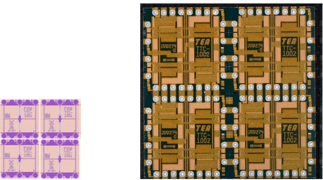
TTCs can accurately simulate the non-uniform power distribution (“hot spots”) of a real semiconductor chip, with embedded on-chip sensors for real-time and accurate temperature measurement of the chip, providing the capability for configurable power distribution and in situ temperature measurement on the chip – down to the scale of a Unit Cell (1mm x 1mm)
Critical technical considerations include uniformity and matching across the wafer, and constant power dissipation throughout the thermal measurement, for the heat source. Conformance to the JEDEC JESD51-4 standard is also a very important requirement. Another important consideration is the Temperature Sensing Diodes (TSD), less than 35µm in dimension, for real-time precise measurement of the temperature of the die at multiple locations simultaneously.
Versatile, stable, and accurate TTCs can be a reliable thermal twin of various semiconductor chips, from chiplets as small as 1mm x 1mm to large chips and interposers (up to 50mm x 50mm, or larger if needed). The TTC, with its precision and accuracy of the integrated heaters and sensors in each Unit Cell, can accurately simulate the thermal behavior of a real semiconductor chip and thereby offers a great tool for concurrent development of thermal management solutions while a new chip is under development (which often takes several years).
A TTC can have multiple heating zones and temperature sensors, each independently controlled and monitored, to emulate the thermal behaviors of the various functional blocks in a real chip. Figure 2 shows an example of the TTC with non-uniform heating. At the same time, the TTC is easy to operate and use, as its sole function is to simulate the power distribution and measure the temperature across the chip in real-time, without the other functions of a real chip that are not needed for this purpose.
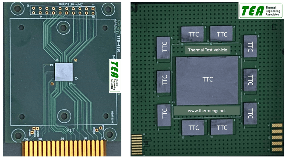
With the TTCs (designed for wire bonding or flip chip attachment), TTVs (Figure 3) can be developed in various packaging formats, such as BGA, LGA, COB, etc., as well as multi-chips per package to simulate system-in-package (SiP) that is often used for heterogeneous integration. TTCs can also be configured for advanced packaging, such as multi-die stacking, glass interposer, etc.
Using the TTCs and TTVs to perform thermal measurements and testing in real real-life environment (i.e., using real-life TIMs and cooling solutions), the spatial and temporal temperature distribution over the chips can be characterized, and the thermal performance of the entire package can be assessed, with high fidelity and confidence.

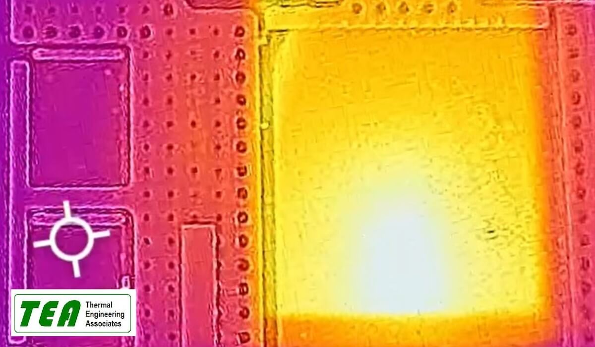
For example, a TTV can be used for TIM thermal characterization under application-oriented measurement conditions (Figure 4).
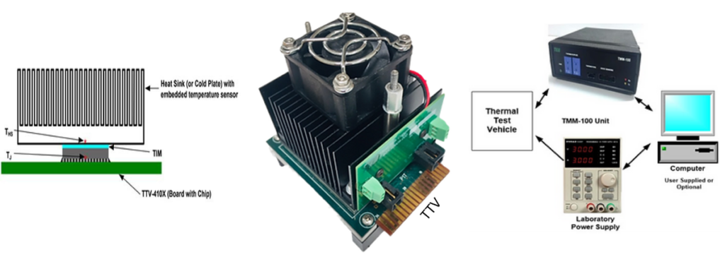
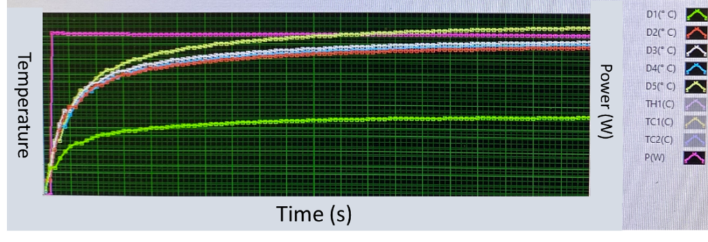
Figure 5 shows an example of the temperature evolution at several locations across a chip when the TTC is powered at a specific power level. Based on the measurement, the thermal impedance and resistance of the package using various thermal management solutions can be calculated. The availability of these tools creates a de facto standard that enables both TIM manufacturers and TIM users to compare measurement results under the same conditions.
Thus, with the ability for configurable power distribution and simultaneous temperature measurement across the chip, TTCs and TTVs can be very useful for thermal characterization (steady state and transient) and evaluation, including power and/or temperature mapping, for semiconductor packages and devices, which can incorporate various thermal management solutions. They can also be very useful for validating thermal simulation and modeling.
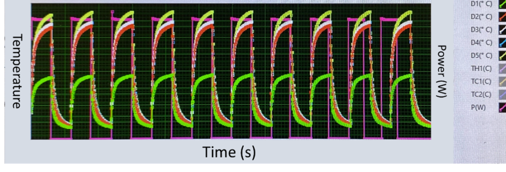
Furthermore, power cycling can be done in a programmed setting to evaluate the reliability performance of various thermal management solutions. Figure 6 is an example of the temperature evolution at several locations in a chip during power cycling. With this configuration, pump-out can be studied in the power cycling setting. TIMs with defects can also be studied for their impact on thermal performance for real-life applications.
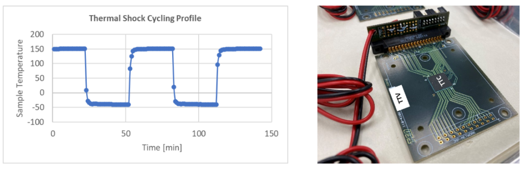
Of course, the TTVs themselves have to be reliable. Recent testing by a large U.S.-based company has demonstrated the reliability of the TTVs through 1000 cycles of -40C/150C thermal shock testing (Figure 7).
With the ability to use TTVs as a de facto standard tool, thermal management solutions can be optimized in fast iterations, in a real-life environment. Such characterization can be done using different size TTCs and at different power levels to assess the performance for different applications. The same TTV can be used many times to make the testing results comparable and objective.
More importantly, with a TTV, developers of thermal management solutions – in industry and academia – can develop the next generation of materials and cooling solutions, by using the TTV at a power level that has not yet been realized in real chips, thus enabling innovation for the future.
Overall, TTCs and TTVs are great tools to enable the rapid development and optimization of thermal management solutions, ultimately ensuring the thermal integrity of semiconductor devices, reliably and cost-effectively.
For more information, please contact Dr. Dongkai Shangguan dongkai@thermengr.com.