Interconnect reliability is critical to the reliability of semiconductor packaging and electronic systems.
If we look at the life cycle from the chip to the system—from IC design, wafer fab, and packaging, to board assembly and system integration—the common element is the “interconnect thread” for the reliability of the electronic system in the field. The primary purpose of semiconductor packaging is to generate interconnects from the chip to the system at different levels: from the die to the substrate, to component termination, and then to the PCB and the system, including various forms of interconnects, such as redistribution layers (RDL), through silicon vias (TSV), wire bonding, solder joints, bumps/balls, direct Cu bonding, and so on. It can also be through photonics (instead of electronics). At the system level, interconnects such as connectors, fibers, and cables, play important roles in the reliability of the electronic system.
Essentially, semiconductor packaging creates interconnects along the signal chain from the IC to the system, for signal and power distribution. Over the past six decades, semiconductor packaging has evolved with the overall trend for ever-shorter interconnects. “Less is Moore”—Miniaturization is good for performance, power, area, cost, and reliability (PPACR).
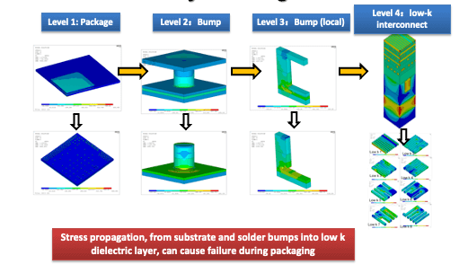
For interconnect reliability out of the chip into the package, we need to first consider chip package interactions (CPI), as low-k dielectrics, used for the electrical performance of the chip, have inferior mechanical properties. When the chip goes through various packaging steps, the mechanical stress generated can propagate to the chip, causing misalignment, deformation, and dielectric fracture. To manage the CPI problem, we need to assess the stress propagation from the substrate and the solder bump into the dielectric layer in the chip, through multi-level multi-scale modeling (Figure 1).
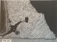
For solder interconnect reliability, we need to look at various cyclic loading conditions — such as thermal cycling, which leads to low cycle fatigue through creep-fatigue interactions, and cyclic bending and vibration which leads to high cycle fatigue — causing solder joint failures through crack initiation and propagation (Figure 2). We also need to look at dynamic mechanical loading conditions such as drop and mechanical shock, which can cause high-frequency flexing of the substrate and fracture of the solder joint. The important factors to consider for dynamic mechanical reliability include strain rate dependency, stress concentration, and interfacial intermetallics (IMC).
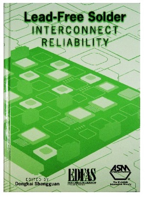
While the lead-free SAC (Sn/Ag/CU) alloys can meet the requirements of many applications, they fall short when it comes to high-stress levels, as the creep strain rate of SAC increases with stress and exceeds that for SnPb at certain high-stress levels. These high-stress levels can arise due to a high coefficient of thermal expansion (CTE) mismatch, a large thermal cycle range, a large component size, or a low stand-off height. More details can be found in the book “Lead-Free Solder Interconnect Reliability” (Figure 3).
Within this background, a new solder system has been developed with enhanced reliability through precipitation hardening and solution hardening, and the solder paste has been formulated with very low voiding. It is considered a “drop-in” solder solution because the reflow process is very similar to the SAC process. This new material has demonstrated superior reliability performance by delayed crack initiation and slow crack propagation in the solder interconnect during thermal cycling.

Often, a low soldering temperature may be needed to reduce the thermal impact on the components and to reduce the warpage of the substrate, which can cause many quality problems. There are also situations where a low-temperature solder is needed for a hierarchical process known as “step soldering.” A low-temperature solder can also help reduce energy consumption during the assembly process. Existing low-temperature alloys (such as SnBi) have exhibited poor performance in drop shock tests due to brittleness. A new material has been developed for reflow at a peak temperature of 200‒210oC, with superior performance under thermal cycling and mechanical shock.
In addition to mechanical loading, electrical loading can also create interconnect reliability problems. Electromigration can take place under an electrical current leading to interconnect failures (Figure 4), and certain solder alloys (such as SnBi) are known to be prone to electromigration. This is becoming more concerning as the electrical current density increases in a miniaturized interconnect.


Sometimes, failures occur not because of the absence of an intended interconnection, but the presence of an unintended one. One such example is a tin whisker (Figure 5), a spontaneous filament that grows very slowly but can cause a failure several years later.
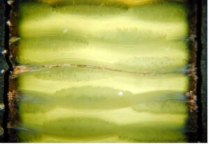
Figure 6. Conductive anodic filament (CAF) in a PCB
Another failure that can occur is a conductive anodic filament (CAF) in a PCB or substrate, where a copper filament (Figure 6) grows under an electrical bias from one via to a neighboring via through the gap between the glass fiber and the epoxy resin with moisture condensation. Similarly, dendrites (Figure 7) can grow through electrochemical migration in the presence of flux residues (which provide ionic contamination) under an electrical bias, thus causing a “short″ in an electrical circuit.
As we enter the era of 5G and 6G, the impact of flux residue on the signal integrity of a circuit at high frequencies is of particular interest. Flux residue can provide an alternative path to signals at a high frequency (Figure 8), and the impact of the flux residue on signal integrity is very sensitive to the presence of moisture. This and other considerations are driving the development of ultra-low residue (ULR) no-clean flux formulations that are adequate for wetting but have a much-reduced impact on the circuit, and these are also compatible with molding and underfill without cleaning.

A very exciting development for fine pitch interconnects (below 10µm) is direct copper interconnection, such as “hybrid bonding.” This process offers superior interconnect reliability as well as signal integrity due to low insertion loss because of a short interconnect path.
As electronic products become more pervasive in applications, interconnect reliability must be considered holistically with regard to environmental conditions—from mechanical and thermomechanical, to electrical and electrochemical—which give rise to different failure modes and mechanisms. The growing adoption of heterogeneous integration leads to an increased diversity of interconnects (with different geometries, materials, and interfaces) in the same package, along with complex (and often interactive) reliability failure modes and mechanisms. These considerations will impact reliability engineering for semiconductor devices, including design, materials, processes, and testing.
For more information, please contact Dongkai Shangguan at dksg@indium.com. (More details can also be found in my invited keynote at the 2022 IEEE Symposium on Reliability of Electronics Packaging & Photonics.)