
 Last week at IWLPC, keynote speaker, Doug Yu, TSMC, kicked off the event with a similar storyline used by ASE’s Tien Wu during his IMAPS Symposium keynote earlier this month:
High-performance applications like artificial intelligence (AI), 5G, autonomous driving, and even high-end smartphones are driving the continuation of Moore’s Law augmented by More than Moore. This need for high-performance technology will benefit the entire semiconductor industry.
Both Yu and Wu told the story of the widening interconnect pitch gap caused by transistor nodes scaling faster than systems. The each offered advancements in fan-out technology (TSMC’s InFO and Deca Technologies’ M-Series) as ways to bridge the gap.
This time, however, the story had a surprise ending.
In Wu’s story, the superhero who saves the day is high-density advanced packaging, where we need to focus our innovation.
In Yu’s story, the superhero is a new character called wafer level system integration (WLSI), and its sidekicks, the Super Acronyms that spell 3D innovation in the front-end.
Super Acronyms to the Rescue
It’s a bird, it’s a plane, it’s SoIC, FE 3D, and BE 3D…
First, a glossary of terms:
- System on Integrated Chips (SoIC) is a vertically integrated, high-density, multi-functional stacked IC.
- Front-end 3D (FE 3D) refers to using front-end processes to build ultra-high density die stacks using high-performance power bonding. FE 3D eliminates the need for micro bumps.
- Back-end 3D (BE 3D) refers to traditional 3D stacking that uses conventional through silicon via (TSV) interconnects, polymers, molding compounds, copper pillars, and micro-bumping.
- Integrated Fan-out (InFO) is TSMCs integrated fan-out technology and claims to be the first high-density 2D/3D fan-out wafer level package (FOWLP).
- Chip-on-wafer-on-substrate (CoWoS) is the industry’s first 2.5D interposer technology
SoICs are built using FE 3D processes and can comprise mixed nodes, active and passives, III-V materials, and even memory, says Yu. SoICs can eventually achieve sub-micron density, unlike 3D ICs, which only achieve multi-micron density with C4 or micro-bumps.
After dicing, SoICs can be integrated via BE 3D in InFO or CoWoS packages. It is a drop-in replacement for system-on-chip (SoC). SoIC is not to be confused with monolithic 3D.

“SoIC is more powerful than people can imagine,” says Yu “Vertical face-to-face stacking offers more direct communication than side-by-side, reducing parasitic. Therefore, SoIC offers both a power and performance advantage over both InFO and CoWos,”
Are You Ready for the 3rd Dimension?
Wu provided the following 3D system integration technology (3D SiT) benchmark slide to compare the benefits of 3D IC, monolithic 3D (M3D) and SoIC. Essentially, he says SoIC offers the benefits of both 3D IC and M3D without the shortcomings of either.
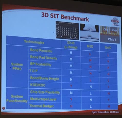
By combining complimentary FE 3D and BE 3D approaches through WLSI, Wu says for the first time in history, system interconnect scales at a pace exceeding Moore’s Law chip scaling.
“Wafer is our business,” says Yu. “WLSI invigorates the supply chain.”
The Role Played by EDA Tools
The second keynote speaker, Mentor’s Wally Rhines said the one thing Yu didn’t mention in his talk is that the industry is on the cusp of a ramp-up. In the past 18 months, CoWoS, InFO and others have taken off, and EDA vendors have been inundated with requests for help in design and verification to take on the next discontinuity in packaging, he said.
“Heterogeneous Integration package design should be easy, but we’re dealing with disparate design teams that are working with different…” tools, processes, die, substrate materials, data output, operating systems… In other words, it’s complicated, and becoming more so as pin counts and package complexity increases.
To report on Rhines’ talk, which attempted to demystify package design to a roomful of packaging engineers, I’ll hand things off to Herb Reiter, our EDA expert, who will write the EDA perspective of IWLPC. Stay tuned!


